'Stamped Grounding Hardware for Electronics'
Short answer: stamped grounding hardware is the small metal parts — clips, spring fingers, serrated washers and screw lugs — that tie a PCB, chassis or shield to a common ground. Their job looks trivial but the electrical requirement is strict: keep contact resistance low and stable, typically under about 10 milliohms per joint, across temperature, vibration and corrosion over the life of the product. The parts that fail EMC or safety tests are rarely the expensive ones. They are the cheap stamped contact that lost normal force or corroded at the interface.
Grounding is where mechanical design and electrical performance collide. A clip that looks fine on a drawing can pass continuity on the bench and still fail salt spray, or lose contact force after vibration and open a safety ground path. This guide covers what stamped grounding parts do, which materials and plating hold low resistance, and how to design and test the joints for the real world.
Why Grounding Hardware Matters in Electronics
A grounding joint serves three different masters. For safety, it provides a low-impedance fault-current path so a short trips the breaker instead of energizing a chassis. For EMC, it gives high-frequency return currents a controlled path so they do not radiate. For ESD, it bleeds static charge to a defined reference without damaging sensitive components.
Each purpose has a different tolerance for resistance. A safety ground must survive repeated fault current; an RF ground must be low-impedance at hundreds of MHz, which depends on geometry as much as on material. That is why a grounding clip is a precision stamped part, not a bracket: the contact force, contact area and plating all set the resistance, and all three degrade with corrosion and mechanical relaxation.
Types of Stamped Grounding Parts
The stamped grounding family is broader than most BOMs suggest.
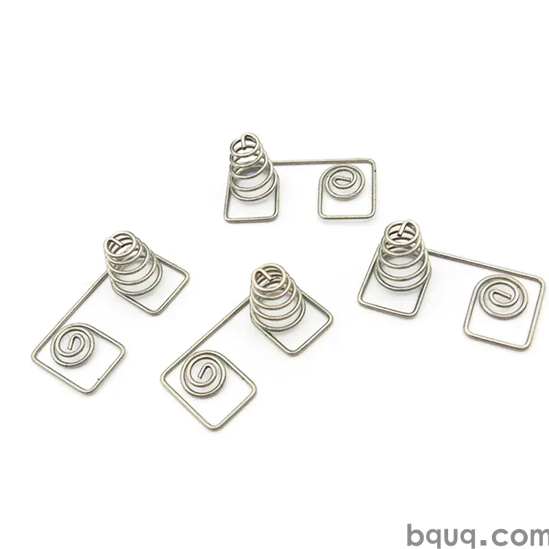
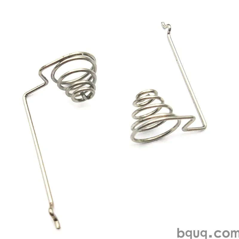
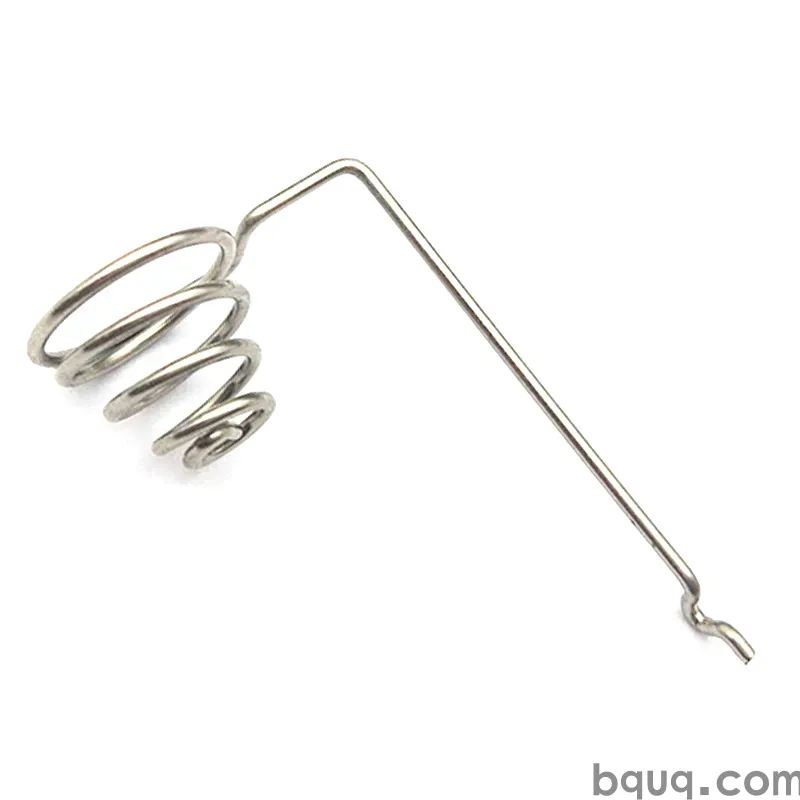
Spring fingers are cantilever or U-shaped contacts that press a board pad or chassis rail to create a compliant ground. Single and double fingers trade contact force against insertion effort. Serrated washers — star, internal-tooth or external-tooth — bite through oxide and paint to reach bare metal under a screw head. Grounding clips hold a shield can or a metal housing down while also grounding it. Screw lugs and grounding plates provide a bolted interface for a ground stud. EMI fences and board-level gaskets form a continuous conductive perimeter around a noisy section. Chassis standoffs with a conductive tip both locate and ground a board.
Because these parts often coexist on the same assembly, it usually pays to stamp the whole family on shared tooling, which is why buyers often source stamping terminals and contacts together with their shield and enclosure parts.
Materials and Plating for Low Contact Resistance
The base metal decides conductivity and spring properties; the plating decides what happens at the interface.
| Finish | Typical contact resistance | Corrosion resistance | Solderability | Typical use |
|---|---|---|---|---|
| Matte tin over nickel | Low, stable | Moderate | Excellent | Solder-down grounds, high volume |
| Bright tin | Low initially | Lower; whisker risk | Good | Cost-driven solder joints |
| Nickel (bare) | Low to moderate | Good | Poor without flux | Wear surfaces, screw interfaces |
| Nickel + gold flash | Very low, very stable | Excellent | Good | Low-level signal and RF grounding |
| Silver | Lowest | Poor without overplate | Good | High-current contacts, not exposed |
| Zinc / chromate on steel | Moderate | Good | Not solderable | Chassis-to-chassis bonding |
For a solderable board ground, matte tin over a nickel barrier is the default. For a screw-tightened or repeatedly mated joint, a nickel underplate with a thin gold flash keeps resistance low and stable and resists fretting. Do not specify gold across an entire washer or clip — restrict it to the contact zone, because gold cost is driven by area. The plating for stamped contacts piece explains how to choose between tin, nickel and gold by interface type.
Designing for Contact Resistance and Retention
Resistance is not one number; it is a stack of bulk resistance, constriction resistance at the contact spots, and film resistance at the surface. You control the last two through normal force, contact geometry and plating.
| Design parameter | Typical target | Why it matters |
|---|---|---|
| Normal force per contact | 0.5-3 N | Enough to break films and stay mated; too much deforms the chassis |
| Contact resistance per joint | < 10 mΩ | Keeps fault current and RF return paths low-impedance |
| Wipe distance on mating | 0.3-1.0 mm | Cleans oxide off the contact spot on insertion |
| Mating cycles | 10-100 for service parts | Sets the temper and plating choice |
| Operating temperature | -40 to +105 °C | Drives stress relaxation and plating choice |
Spring fingers should be made from a spring-temper alloy — phosphor bronze or a copper-beryllium grade — and formed so the finger operates in a deflection range that keeps stress below the material's yield. A finger that is over-deflected at assembly will relax and lose force within a few thermal cycles. Give the mating surface a defined wipe so the contact spot self-cleans, and avoid designs where the finger contacts the same spot every cycle with no sliding action.
Testing and Quality Checks
Contact resistance is measured with a four-wire (Kelvin) method to remove lead resistance, typically reporting milliohms at a specified test current. Mating-force and retention tests confirm the finger delivers the designed normal force. Salt spray and mixed-flowing-gas tests check corrosion behavior of the plating. Vibration and thermal cycling check that the joint stays low-resistance after mechanical and temperature stress.
At BQUQ we ship stamped grounding parts with dimensional inspection data by default and can add contact-resistance or plating-thickness checks to the quality plan. For the full picture of how stamped contacts are inspected, the grounding clips and EMI shielding contacts guides cover the geometry and test angles.
Frequently Asked Questions
Q: What contact resistance should a grounding joint have?
A: For most electronic grounding joints, target under about 10 milliohms per interface, measured with a four-wire method. RF grounds often need lower and more stable resistance, which usually means a nickel underplate with a gold flash on the contact zone rather than bare tin.
Q: Which plating is best for a grounding clip?
A: It depends on the interface. For a soldered ground, matte tin over nickel is the standard and cheapest reliable option. For a screw or repeatedly mated joint, a nickel underplate with a thin gold flash keeps resistance low and stable and resists fretting corrosion. Bare nickel is a good wear surface but hard to solder.
Q: Why does a grounding clip lose contact after a few months?
A: Usually stress relaxation or corrosion. A finger that is over-deflected at assembly gradually loses normal force, and the contact spot develops an oxide or corrosion film. Fix it by designing the finger to operate within its elastic range, adding wipe on mating, and choosing plating suited to the environment.
Q: Can stamped grounding parts be made to a tight tolerance?
A: Yes. Grounding clips, fingers and washers are stamped to ±0.05 mm on critical features as a standard, with tighter control where a specific contact height or finger position demands it. Because these parts control electrical performance, we treat the contact-critical dimensions as key characteristics on the inspection plan.
Q: What is the lead time and MOQ for stamped grounding hardware?
A: There is no fixed MOQ; the practical minimum depends on tooling. Soft or bridge tooling supports low-volume runs, while progressive dies serve high volume. Send the drawing with material, plating and quantity to sc@bquq.com and BQUQ returns an indicative quote within 12 working hours.
Related Resources
- Stamped Grounding Clips: geometry and design notes for clips that also carry ground current.
- Terminals and Contacts: stamped contact and grounding parts made on progressive dies.
- About BQUQ: an ISO9001-certified source factory in Dongguan running stamping, CNC, springs, collets and heat sinks under one roof.
- Contact us: send your drawing to sc@bquq.com for a quote within 12 working hours.
Authored by the BQUQ Engineering Team. BQUQ is an ISO9001-certified source factory in Dongguan, China, running CNC machining, metal stamping, custom springs, heat sink and collet lines under one roof. Send drawings to sc@bquq.com or WhatsApp +86 13713157787 for a quote within 12 working hours. www.bquq.com