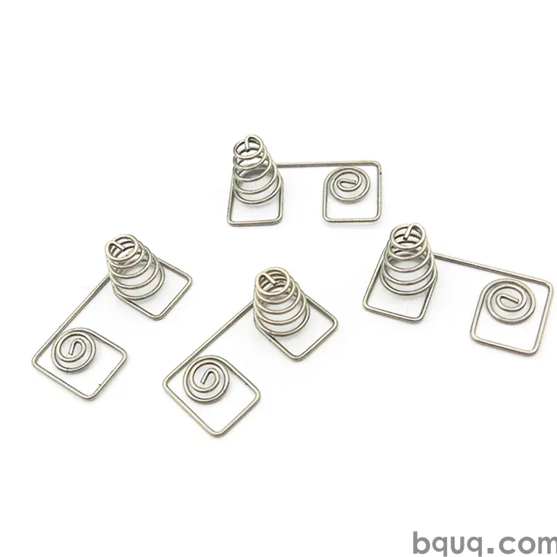
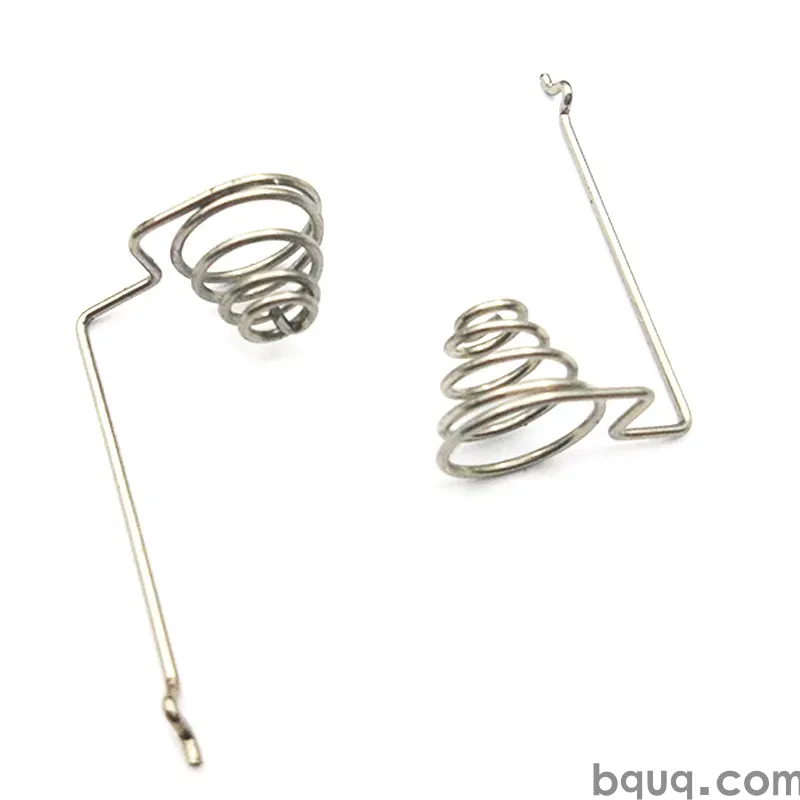
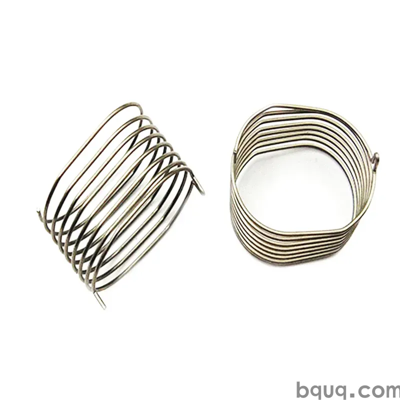
Stamped terminal and contact design rules: alloys, bend radius, contact force, plating and tolerances for thousands of reliable cycles.
Stamped Terminals and Contacts: Design Rules for Reliability
A stamped terminal or contact fails in one of three ways: the metal fatigues and loses spring force, the plating wears through at the contact zone, or the geometry drifts enough that insertion force or mating position goes out of spec. All three are design decisions made before the die exists — material grade, bend radius, contact pressure, and plating thickness. Get those right and a stamped contact reliably survives thousands of cycles; get them wrong and no amount of manufacturing care will fix it.
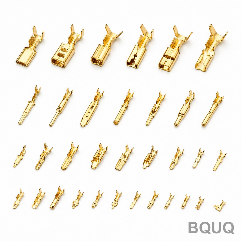
Terminals and contacts are the precision end of metal stamping: connector pins, crimp terminals, socket contacts, fuse clips, and the spring contacts behind switches and battery holders. They are stamped from thin copper-alloy strip, often 0.05–1.0 mm thick, and their reliability depends on a handful of mechanical and electrical rules that this guide sets out in engineering terms.
Start with the Right Copper Alloy
Contact reliability begins with material choice because the metal is doing two jobs at once: carrying current and acting as a spring. Pure copper conducts superbly but has almost no springiness, so terminals use copper alloys that trade a little conductivity for a lot of elastic strength. The alloy's yield strength decides how much contact force the design can sustain without taking a permanent set, and its fatigue strength decides how many insertion or flexing cycles it survives.
| Alloy | Conductivity (typical, % IACS) | Why it is used |
|---|---|---|
| Brass C2600/C2680 | ~28 | Cheap terminals, low cycle counts |
| Phosphor bronze C5191/C5210 | ~15–20 | Reliable spring force, good fatigue life |
| Beryllium copper C17200 | ~20–25 | Highest cycle life, strongest spring per size |
| Copper-nickel-silicon (C7025) | ~40–50 | High current plus springiness, costlier |
| Stainless 301 (spring temper) | ~2–3 | Corrosion resistance, low conductivity |
The takeaway: match alloy to cycle count and current, not to habit. A battery contact flexed tens of thousands of times in a consumer product needs beryllium copper or a high-performance substitute; a one-time crimp terminal can be plain brass. Material cost differences are small per part but large in reliability.
Bend Radius and Forming Rules That Prevent Cracking
Stamped contacts are bent from strip, and every bend is a place where the material has been cold-worked past its elastic limit. Bend along the rolling direction of the strip is the risky orientation — if the inside radius is too sharp, the outside surface cracks because it must stretch further than the alloy allows. The standard rule is an inside radius of at least one material thickness for most copper alloys, and more for hard-tempered material.
Two more forming rules matter for contacts specifically. First, spring contacts rely on a cantilever or beam geometry, so the bend that creates the beam must not be in the highest-stress zone — move the flex point away from the bend heel. Second, avoid sharp transitions in width along the beam; stress concentrates where the section narrows, and a contact that breaks after 5,000 cycles instead of 50,000 is usually failing at such a transition. These are exactly the details a good stamping design review catches on the drawing before tooling is cut.
Contact Force: The Number Everything Hangs On
Contact force is the single most important reliability parameter in a stamped contact. It sets contact resistance (higher force, lower resistance), insertion force, and wear life. For signal-level contacts, a normal force of roughly 50–150 grams is typical; power contacts run higher. The force comes from beam geometry, material modulus, and thickness — and it must stay within spec across manufacturing tolerances and temperature.
| Contact parameter | Typical range | What drives it |
|---|---|---|
| Normal force, signal contacts | 50–150 g | Beam length, thickness, material |
| Insertion force per contact | 150–500 g | Contact geometry, plating friction |
| Contact resistance target | 10–50 mΩ | Force, plating, surface finish |
| Rated insertion cycles | 500–10,000 | Alloy fatigue, plating wear-through |
Two reliability traps follow. First, contact force decays with insertion cycles as the beam takes a small permanent set — design the initial force high enough that it stays above the minimum at end of life. Second, do not push force arbitrarily high to fix resistance: force and insertion force rise together, and an operator fighting a 500-gram connector is a quality complaint waiting to happen.
Plating: Thin Where It Is Cheap, Thick Where It Counts
Plating on a stamped terminal has one main job at the contact zone — keeping the interface clean and low-resistance — and a secondary job elsewhere, solderability or corrosion protection. The economical pattern is selective plating: gold or silver only where the electrical contact actually wipes, tin over the rest. Gold thickness at the contact zone typically runs 0.1–0.76 µm for moderate cycle counts and up to ~1.5 µm for high-reliability or high-cycle designs; tin plating runs 1–8 µm.
Plating failures are almost always wear or porosity, not the plating itself. A contact rated for 10,000 insertions with 0.1 µm of gold will fail early because the gold wears through and the base metal oxidizes. Under-plating at the contact zone is the classic cost-cutting mistake; over-plating everywhere else is the classic over-engineering one. Specify thickness by zone — contact area, solder tail, and body can legitimately carry three different plating specs.
Tolerances and Feature Design That Stamp Well
Terminals and contacts are small, so their tolerances are tight, but they must be tolerances stamping can actually hold. Critical width and pitch dimensions hold ±0.02–0.05 mm in a well-built progressive die. Bend angles run ±0.5–1°, which matters for contact position at the mating end. If the design needs better than that, the fix is usually a coining station or a post-stamping operation, both of which add tooling cost — the detail is covered in our metal stamping tolerances guide.
| Design feature | Rule of thumb |
|---|---|
| Minimum feature width | ≥ 1× material thickness |
| Hole-to-edge distance | ≥ 1× thickness (cut quality) |
| Inside bend radius | ≥ 1× thickness |
| Slot width | ≥ 0.8× thickness, tooling dependent |
| Pitch between terminals | Hold ±0.02–0.05 mm with piloting |
These minimums exist because stamping is shearing and bending, not machining. Features smaller than the material thickness make fragile punches that break, and edges closer than one thickness to a hole distort the hole. Respect the minimums and the die runs millions of strokes; ignore them and you buy replacement punches instead of parts.
Email sc@bquq.com or WhatsApp +86 137 1315 7787 with your PDF/DXF/STEP file. An engineer reviews it and replies with price, lead time and DFM notes on working days.
Frequently Asked Questions
Q: What is the best material for a high-cycle stamped contact?
Beryllium copper C17200 gives the best spring force and fatigue life per unit of size, which is why it dominates high-cycle touch and battery contacts. Phosphor bronze is the economical choice for moderate cycle counts, and copper-nickel-silicon alloys suit higher-current applications.
Q: How thick should gold plating be on a contact?
For the contact zone, 0.1–0.4 µm gold is typical for moderate duty, rising toward 0.76–1.5 µm for high-cycle or high-reliability designs. Tin, where used, runs 1–8 µm. Specify thickness by zone rather than one value for the whole part.
Q: What contact force should I design for?
Signal-level contacts typically use 50–150 g normal force; power contacts need more. Size the initial force so it stays above the required minimum after thousands of insertion cycles, and watch that insertion force stays acceptable to the end user.
Q: How tight can stamped terminal dimensions be held?
Critical width and pitch dimensions hold ±0.02–0.05 mm in normal progressive die production; bend angles run about ±0.5–1°. Tighter requirements need coining stations or secondary operations, which raise tooling and piece cost.
Q: When is stamping the wrong process for a contact?
At low volume — below roughly a few thousand pieces a year — the die cost cannot be recovered, and CNC machining, wire EDM, or existing stock contact shapes are cheaper. At high volume and small size, progressive stamping is usually the lowest-cost route there is.
Related Articles
- progressive-die-stamping-cost-guide — More from the BQUQ Metal Stamping engineering series.
- metal-stamping-defects-guide — More from the BQUQ Metal Stamping engineering series.
- stamping-die-maintenance-guide — More from the BQUQ Metal Stamping engineering series.
Data Sources and Verification
Tolerances, cycle times and price ranges in this guide come from BQUQ production records at our Dongguan plant, where CNC machining (±0.005 mm), stamping, custom springs and heat sinks run under one roof. BQUQ is an ISO 9001:2015 certified factory; the certificate and batch inspection reports are available on request with every quotation.
Related Resources
- About BQUQ: an ISO9001-certified source factory in Dongguan running four production lines under one roof.
- Stamping and sheet metal: terminals, brackets and enclosures from the press line — stamped terminals and contacts, stamping brackets and mounts, sheet metal enclosures.
- Industry trends: manufacturing, material market, and sourcing analysis for buyers.
- Technical articles: engineering guides and process comparisons — more where this article came from.
- FAQ hub: quick answers on CNC, stamping, springs, and heat sinks.
- Case studies: real parts and real numbers from projects we engineered and delivered.
- Contact us: send your drawing and get a quote within 12 working hours.
Authored by the BQUQ Engineering Team. BQUQ is an ISO9001-certified source factory in Dongguan, China, running CNC machining, metal stamping, custom springs and heat sink lines under one roof. Send drawings to sc@bquq.com or WhatsApp +86 13713157787 for a quote within 12 working hours. www.bquq.com