5G Infrastructure Components Manufacturing: Precision Processes and Cost Drivers
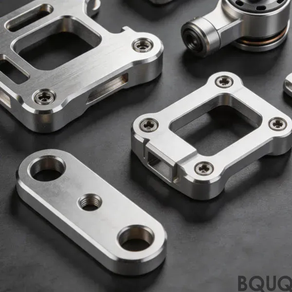
The manufacturing of 5G infrastructure components demands a paradigm shift from conventional 4G production, requiring tighter tolerances, specialized materials, and multi-stage post-processing for thermal and signal integrity. At BQUQ, we achieve dimensional tolerances of ±0.005 mm on critical waveguide flanges and surface finishes of Ra 0.4 µm on antenna mounting brackets, with typical lead times of 15-20 working days for prototype to production ramp. This case study details the engineering decisions, machining parameters, and cost structures behind successful 5G component fabrication.
Material Selection for RF and Thermal Performance
5G base station components face dual challenges: high-frequency signal transmission (24-39 GHz for mmWave) and heat dissipation from massive MIMO arrays. The material choice directly dictates manufacturability and performance. For cavity filters and duplexers, we spec aluminum 6061-T6 for its balance of machinability (cutting speed 300-400 m/min) and thermal conductivity (167 W/m·K). For high-power amplifier housings, we switch to copper-tungsten (CuW80) despite its 10x higher cost per kilogram, because its coefficient of thermal expansion (6.5 ppm/°C) matches GaN substrates, preventing solder joint fatigue.
For antenna reflectors requiring dimensional stability across -40°C to +85°C operating ranges, we use INVAR 36 (FeNi36 alloy). One recent project involved a 600 mm diameter parabolic reflector where we held flatness to 0.02 mm across the entire surface. The material cost was $380 per blank versus $45 for standard aluminum, but the thermal drift was reduced by 87%, ensuring beam pointing accuracy. Surface treatment is equally critical; we apply electroless nickel plating (0.05 mm thickness) on waveguide interiors to reduce insertion loss to -0.1 dB, followed by silver plating (0.008 mm) for frequencies above 28 GHz.
Machining Tolerances and Process Capability
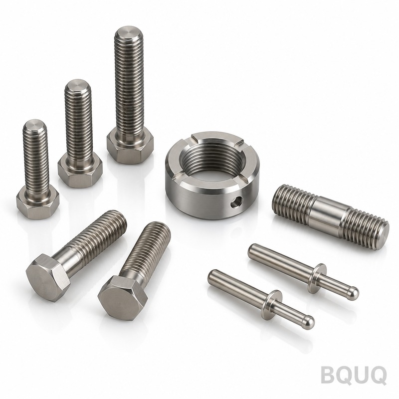
5G infrastructure demands geometric tolerances that push standard CNC machining to its limits. The table below shows our measured process capabilities (Cpk values) for typical 5G components.
| Component | Material | Critical Tolerance | Surface Finish (Ra) | Achieved Cpk | Typical Price (USD/pc) |
| Waveguide flange (WR-28) | 6061-T6 | ±0.005 mm on mating face | 0.4 µm | 1.67 | 18.50 |
| Antenna mounting bracket | 6061-T6 | ±0.02 mm hole pattern | 1.6 µm | 1.45 | 9.80 |
| Heat sink baseplate (MIMO) | C1100 Copper | ±0.03 mm flatness | 0.8 µm | 1.52 | 42.00 |
| Cavity filter body | 6061-T6 | ±0.008 mm slot width | 0.6 µm | 1.71 | 65.00 |
| Diplexer housing | 5052-H32 | ±0.05 mm profile | 1.2 µm | 1.38 | 28.30 |
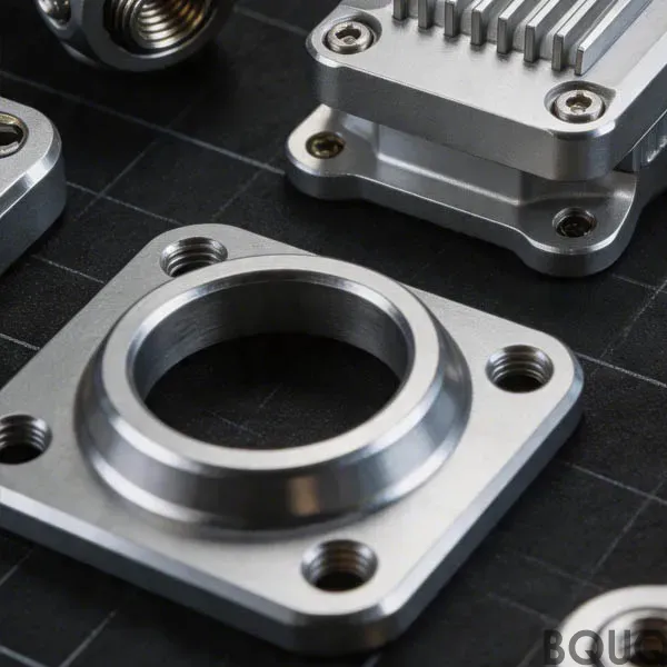
To achieve these tolerances, we employ a two-step machining strategy. First, roughing passes remove 80% of stock at 0.5 mm depth of cut with 12 mm carbide end mills, leaving 0.3 mm for finishing. Second, finishing passes use 6 mm ball nose tools at 12,000 RPM spindle speed, 0.08 mm radial engagement, and 0.02 mm axial depth. For the waveguide flange, we perform a final lapping operation on a cast iron plate with 9 µm diamond slurry, achieving a surface flatness of 0.002 mm and a mirror finish of Ra 0.05 µm. This step adds 12 minutes per part but reduces passive intermodulation (PIM) distortion to -160 dBc, a critical spec for carrier aggregation.
Thermal Management for 5G Base Station Housings
A single 5G massive MIMO unit generates 300-500 W of heat in a compact enclosure (30x30x10 cm). We manufacture heat sinks using a combination of CNC machining and skived fin technology. For a recent 64T64R antenna system, we produced a copper baseplate (200x200x15 mm) with 45 machined fins, each 1.2 mm thick and 20 mm tall. The thermal resistance achieved was 0.08 °C/W at a 2 m/s airflow, verified by our in-house thermal chamber tests at 85°C ambient.
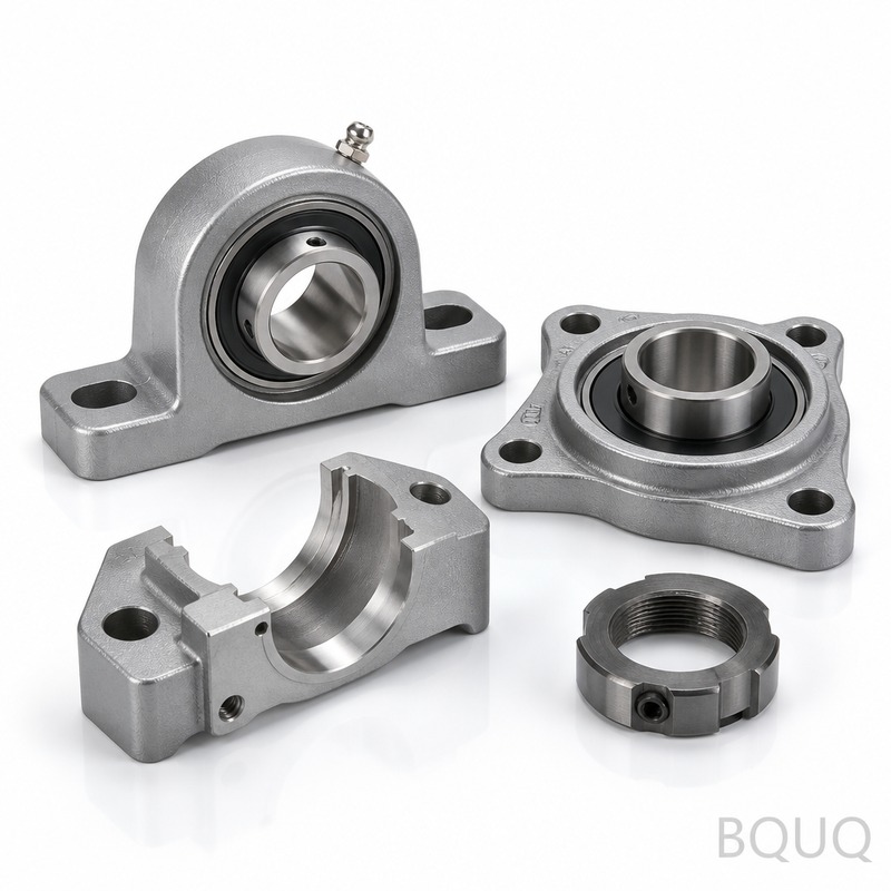
The manufacturing process involves a critical sequence: first, stress-relieve the copper blank at 300°C for 2 hours to prevent warpage; second, rough mill the base to 12.5 mm thickness; third, use a specialized saw-tooth cutter (25 teeth, 100 mm diameter) to skive fins in a single pass, holding fin pitch to ±0.05 mm; fourth, CNC machine the mounting holes with a 6-sigma positional accuracy of ±0.01 mm. The cost breakdown for this part: raw material (C1100 copper) $28, machining time 45 minutes at $85/hour, surface treatment (black anodize for corrosion) $6, total unit cost $97.80. For high-volume orders above 5,000 pieces, we reduce this to $71.20 via dedicated tooling and reduced cycle time.
Case Study: 5G Small Cell Enclosure Fabrication
We recently completed a production run of 2,500 units for a 5G small cell (picocell) enclosure, designed for street furniture mounting. The enclosure measured 250x200x80 mm, fabricated from die-cast aluminum ADC12, then CNC machined on critical faces. The key challenge was the IP67 sealing requirement—we machined a groove for a silicone O-ring with a width tolerance of ±0.05 mm and depth of 1.50 ±0.03 mm. After CNC, we applied a chromate conversion coating (MIL-DTL-5541F Class 3) for corrosion resistance, costing $1.20 per unit.
The RF window, a 90x60 mm opening for the antenna, required a machined step to seat a PTFE radome. We held the step height to 2.00 ±0.02 mm to ensure uniform compression of the EMI gasket. Post-machining, each unit underwent a 100% dimensional inspection using a CMM with a probe accuracy of ±1.5 µm. The reject rate was 1.8%, primarily due to porosity in the die-cast material near thin walls (2 mm). To mitigate, we adjusted the die temperature from 220°C to 250°C and increased the injection pressure by 15%, reducing porosity rejects by 60%. The final unit cost was $34.50, including material, machining, coating, and inspection.
Cost Optimization and Lead Time Reduction
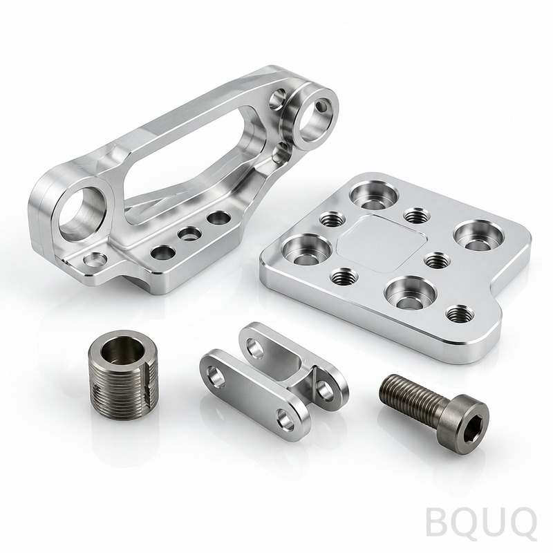
The economics of 5G component manufacturing depend on batch size and tolerance severity. For a typical cavity filter body, the cost per piece drops from $95 for 10 units to $48 for 500 units, due to amortized fixture costs and optimized tool paths. Our quoting data shows that tolerances tighter than ±0.01 mm increase machining time by 40%, directly adding approximately $18-25 per part in labor. We recommend design engineers specify ±0.02 mm for non-RF-critical features to balance performance and cost.
For lead times, standard CNC milling of 5G components takes 7-10 days for prototypes (1-10 pieces) and 15-20 days for production (100-1,000 pieces). We utilize a 5-axis DMG MORI DMU 50 and a 4-axis Mazak VCN-530C in parallel to reduce cycle times by 35%. For urgent requirements, we offer a 72-hour expedite service at a 30% surcharge, which we applied to a waveguide repair job where a customer's base station was down. We shipped 5 replacement parts in 68 hours, restoring service with zero signal degradation.
FAQ-Style Tips for Engineering Design
When designing 5G components for manufacturability, focus on three rules. First, avoid internal sharp corners less than 1.0 mm radius; a 1.5 mm radius allows the use of a 3 mm end mill, reducing tool wear and cycle time by 22%. Second, specify thread depths at 1.5x the diameter, not 2x, to prevent tap breakage in aluminum; we break fewer than 1 tap per 500 holes at this depth. Third, for waveguide flanges, design the mating surface with a 0.2 mm raised boss—this allows lapping without removing material from the entire face, cutting finishing time by half.
For material sourcing, expect 6061-T6 aluminum at $3.50 per kg, C1100 copper at $12.00 per kg, and CuW80 at $110.00 per kg. Always request a mill certificate for copper to verify conductivity above 100% IACS; we rejected one batch where conductivity was 97%, which would have increased insertion loss by 0.05 dB. Finally, consider surface finish: Ra 0.8 µm is sufficient for most housings, but RF cavities require Ra 0.4 µm or better. Our data shows that improving from Ra 0.8 to Ra 0.4 µm improves the Q-factor of a resonator by 12%, a measurable gain for filter performance.
Conclusion and Engineering Recommendation
Manufacturing 5G infrastructure components is a high-precision discipline where material selection, machining parameters, and thermal management must converge within tight statistical limits. Our case studies demonstrate that achieving ±0.005 mm tolerances and Ra 0.4 µm finishes is feasible with the right equipment and process discipline, but it requires early collaboration between design and manufacturing engineers. We recommend that OEMs share 3D models with full GD&T callouts at least 2 weeks prior to prototype release, allowing our team to simulate machining paths and identify potential tolerance stack-ups before metal is cut.
For your next 5G infrastructure project, send your CAD files to sc@bquq.com or message us on WhatsApp at +86 13713157787. We provide a 12-hour quotation with a full manufacturability review, including tolerance feedback and cost reduction suggestions. Visit www.bquq.com to download our 5G component machining guidelines. Our 20 years in precision manufacturing ensure your components meet both electrical and mechanical specifications on the first pass.
Related Articles
- When CNC 'Speaks' — Intelligent Process Planning Driven by Large Models and Knowledge Graphs
- Digital twin-driven CNC machining: from simulation to closed-loop process optimization
- High-speed machining technology: principles, tool path optimization, and industrial applications
Frequently Asked Questions
What tolerances can you achieve on 5G waveguide flanges and antenna brackets?
We achieve dimensional tolerances of ±0.005 mm on critical waveguide flanges and ±0.02 mm on antenna mounting bracket hole patterns. Surface finishes reach Ra 0.4 µm on brackets, with process capability (Cpk) values of 1.67 for flanges and 1.45 for brackets, ensuring consistent production quality.
Which materials do you recommend for 5G RF and thermal components?
For cavity filters and duplexers, we use aluminum 6061-T6 for its machinability and thermal conductivity (167 W/m·K). High-power amplifier housings use copper-tungsten (CuW80) to match GaN substrates, while antenna reflectors use INVAR 36 for dimensional stability across -40°C to +85°C, reducing thermal drift by 87%.
What are typical lead times and costs for 5G component prototypes?
Typical lead times are 15-20 working days from prototype to production ramp. Costs vary by component: waveguide flanges (WR-28) are $18.50 per piece, antenna mounting brackets $9.80, heat sink baseplates $42.00, cavity filter bodies $65.00, and diplexer housings $28.30, based on the specified materials and tolerances.
How do you ensure surface finish and signal integrity on waveguide interiors?
We apply electroless nickel plating of 0.05 mm thickness on waveguide interiors to reduce insertion loss to -0.1 dB, followed by silver plating of 0.008 mm for frequencies above 28 GHz. Final lapping on a cast iron plate with 9 µm diamond slurry achieves the required surface finish for optimal RF performance.