CNC Machining Precision for Semiconductor Equipment
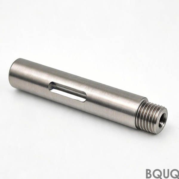
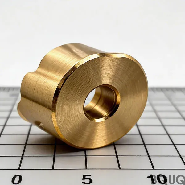
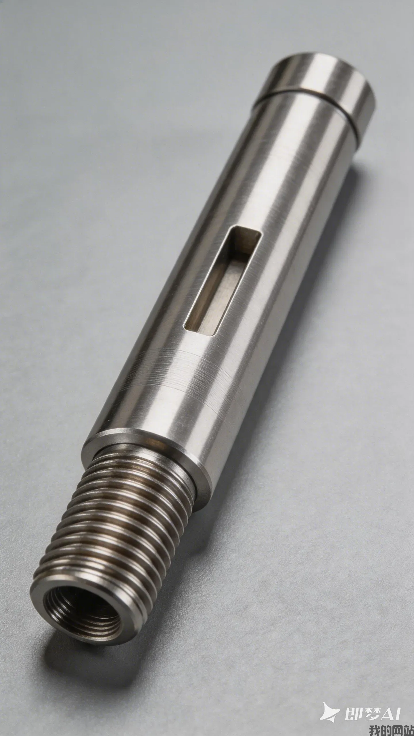
In the semiconductor industry, precision is not just a goal—it is a necessity. As chip designs shrink to nanometer scales, the equipment used to manufacture them must operate with extraordinary accuracy. CNC machining plays a pivotal role in producing critical components for semiconductor fabrication equipment, from wafer handling robots to deposition chambers. This guide explores the stringent precision requirements and best practices for CNC machined parts in semiconductor applications.
The Critical Role of Precision in Semiconductor Manufacturing
Semiconductor manufacturing involves processes like photolithography, etching, and deposition, all of which demand near-perfect alignment and repeatability. A deviation of even a few microns can render a wafer useless. CNC machined components—such as chucks, lift pins, and gas distribution plates—must maintain tolerances as tight as ±0.002 mm. This level of precision ensures consistent performance and minimizes defects.
Key Precision Requirements for CNC Machined Semiconductor Components
Tolerances
Typical tolerances for semiconductor parts range from ±0.005 mm to ±0.001 mm, depending on the application. For example, wafer handling fingers require ultra-precise positioning to avoid scratching or misalignment. Achieving such tolerances demands advanced CNC machines with high-resolution encoders and thermal compensation.
Surface Finish
Surface roughness (Ra) must often be below 0.4 μm to prevent particle generation and ensure proper sealing. Mirror finishes (Ra < 0.1 μm) are common for components in vacuum environments. Polishing, honing, or diamond turning may be used after initial machining.
Material Selection
Common materials include aluminum 6061, stainless steel 316L, titanium, and engineering plastics like PEEK. Each material must be free of internal stresses and impurities to maintain stability during machining and in service.
Cleanliness
Parts must be free of burrs, chips, and contaminants. Often, they undergo ultrasonic cleaning and are packaged in cleanroom conditions to meet ISO Class 4 or better.
CNC Machining Techniques for Achieving Semiconductor-Grade Precision
To meet the demanding requirements, manufacturers employ:
5-axis machining: Allows complex geometries in a single setup, reducing errors from reclamping.
High-speed spindles (30k–60k RPM): Enable fine cuts with minimal tool deflection.
Advanced cooling systems: Maintain thermal stability, preventing expansion that could alter dimensions.
Toolpath optimization: Using CAM software to minimize vibrations and ensure consistent chip loads.
In-process probing: Real-time measurement and compensation for tool wear and thermal drift.
Material Selection and Its Impact on Precision
Choosing the right material is crucial for both machinability and final part performance. Aluminum offers good strength-to-weight ratio and thermal conductivity, making it ideal for heat sinks and chambers. Stainless steel provides corrosion resistance and stiffness for structural parts. Ceramics like alumina are used for electrical insulation but require specialized grinding techniques. Plastics like PEEK are chosen for their chemical resistance and low outgassing. Each material demands specific cutting parameters and tooling to achieve the required precision.
Quality Control and Measurement in Semiconductor CNC Machining
Rigorous inspection ensures parts meet specifications. Common metrology tools include:
Coordinate Measuring Machines (CMM): For dimensional verification with micron-level accuracy.
Laser interferometers: To calibrate machine positioning and verify linear accuracy.
White light interferometry: For surface roughness measurement.
Vision systems: For non-contact measurement of complex features.
Statistical process control (SPC) is used to monitor production trends and maintain consistency.
Common Challenges and Solutions in Semiconductor CNC Machining
| Challenge | Solution |
|---|---|
| Thermal expansion causing dimensional drift | Use temperature-controlled coolant and machine enclosures; pre-warm machine and parts. |
| Vibration leading to poor surface finish | Balance tools, use vibration-damping tool holders, optimize cutting parameters. |
| Tool wear affecting tolerances | Implement tool wear monitoring and automated compensation; choose high-quality carbide or PCD tools. |
| Burr formation | Use specialized deburring tools, apply ultrasonic cleaning, and design tools with proper chip evacuation. |
Choosing a CNC Machining Partner for Semiconductor Applications
When selecting a supplier, consider:
Certifications: ISO 9001, AS9100, and ideally ISO 13485 for medical-grade cleanliness.
Cleanroom capabilities: Class 1000 or better for assembly and packaging.
Experience: Proven track record with semiconductor OEMs and Tier 1 suppliers.
Equipment: Modern 5-axis machines, in-process metrology, and CMM.
Materials expertise: Knowledge of specialty alloys and plastics.
Conclusion
CNC machining for semiconductor equipment requires an unwavering commitment to precision, cleanliness, and quality. By understanding the specific requirements—tolerances, surface finish, material behavior, and contamination control—manufacturers can produce components that enable the relentless advancement of chip technology. Partnering with an experienced CNC machinist who invests in advanced equipment and rigorous quality systems is essential for success in this demanding field.
Frequently Asked Questions
What tolerances can your CNC machining achieve for semiconductor components?
Typical tolerances for semiconductor parts range from ±0.005 mm to ±0.001 mm, depending on the application. For example, wafer handling fingers require ultra-precise positioning to avoid scratching or misalignment. Achieving these tolerances demands advanced CNC machines with high-resolution encoders and thermal compensation.
What surface finish requirements do semiconductor parts need?
Surface roughness (Ra) must often be below 0.4 μm to prevent particle generation and ensure proper sealing. Mirror finishes (Ra < 0.1 μm) are common for components in vacuum environments. Polishing, honing, or diamond turning may be used after initial machining to achieve these finishes.
Which materials do you recommend for semiconductor manufacturing parts?
Common materials include aluminum 6061, stainless steel 316L, titanium, and engineering plastics like PEEK. Each material must be free of internal stresses and impurities to maintain stability during machining and in service, ensuring long-term dimensional accuracy.
How do you ensure cleanliness of machined parts for semiconductor use?
Parts must be free of burrs, chips, and contaminants. They undergo ultrasonic cleaning and are packaged in cleanroom conditions to meet ISO Class 4 or better, ensuring they are suitable for sensitive semiconductor fabrication environments.