Precision Metal Stamping for Electronics: Key Considerations Guide
Introduction
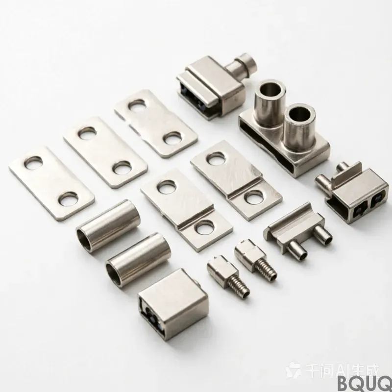
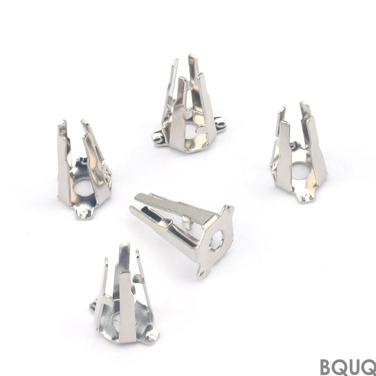
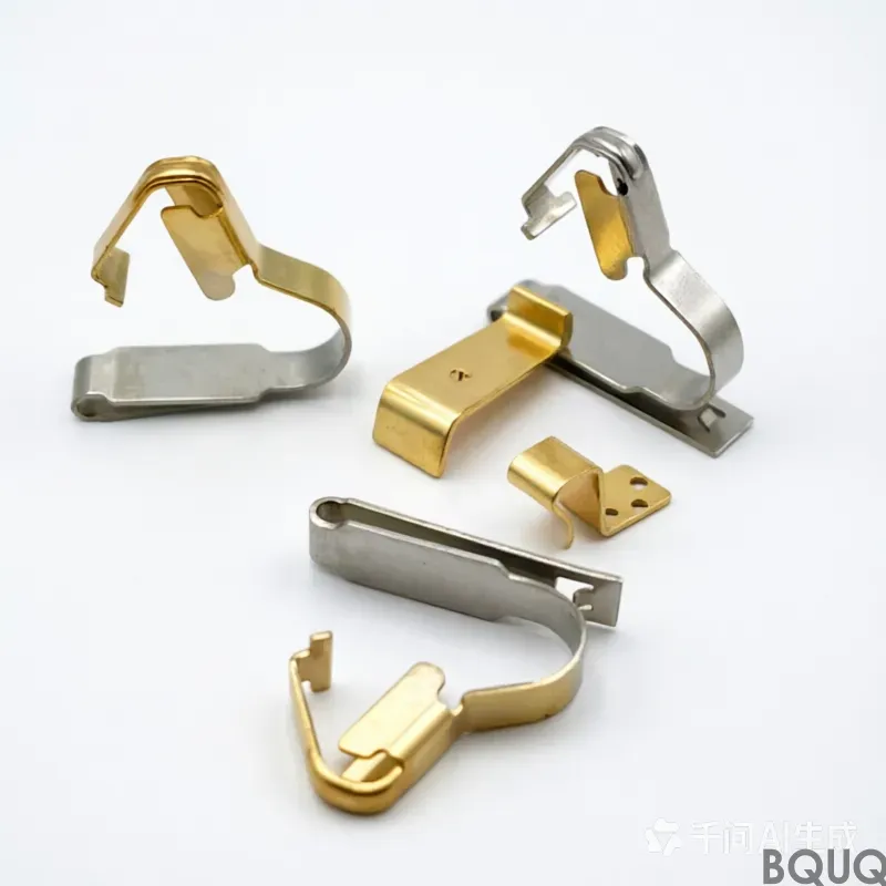
Precision metal stamping is a cornerstone of modern electronics manufacturing, enabling the production of intricate components with tight tolerances at high volumes. From connectors and shielding to heat sinks and springs, stamped metal parts are ubiquitous in devices ranging from smartphones to medical equipment. However, achieving consistent quality and performance requires a thorough understanding of key considerations specific to electronics applications. This guide explores the critical factors that engineers and procurement professionals must evaluate to ensure successful outcomes in precision metal stamping for electronics.
Material Selection: The Foundation of Performance
Choosing the right material is perhaps the most critical decision in metal stamping for electronics. The material must meet electrical conductivity, thermal management, strength, and corrosion resistance requirements while being compatible with the stamping process.
Common Materials and Their Applications
| Material | Key Properties | Typical Electronics Uses |
|---|---|---|
| Copper (C110, C102) | Excellent electrical and thermal conductivity, good formability | Connectors, lead frames, EMI shielding |
| Brass (C260, C268) | Good conductivity, corrosion resistance, easy to stamp | Terminals, sockets, spring contacts |
| Phosphor Bronze (C510, C521) | High fatigue strength, good conductivity | Springs, shrapnel, connectors with repeated bending |
| Stainless Steel (304, 316) | High strength, corrosion resistance, magnetic options | Shielding cans, brackets, structural parts |
| Nickel Silver (C752) | Good spring properties, corrosion resistance, solderable | Miniature connectors, switch contacts |
Tip: When selecting materials, consider the entire lifecycle: formability during stamping, subsequent plating or coating requirements, and performance under thermal cycling in the final device.
Precision Tolerances: From Microns to Success
Electronic components often require tolerances as tight as ±0.025 mm or even finer. Achieving such precision depends on factors like tooling quality, press stability, and material consistency.
Key Tolerance Considerations
Die Alignment: Misalignment of punches and dies can cause burrs, dimensional variation, and premature wear. Precision stamping uses guide pins and progressive dies with tight clearance.
Material Thickness Variation: Incoming material must meet strict thickness tolerances (e.g., ±0.005 mm) to maintain consistent part dimensions.
Springback Compensation: After stamping, materials like stainless steel tend to spring back slightly. Advanced simulation and tool design account for this to ensure final geometry meets specs.
Burr Control: Burrs can interfere with assembly or cause short circuits. Proper clearance and sharp tooling minimize burrs; secondary processes like tumbling may be needed.
Tip: Work closely with your stamping partner to define critical-to-function dimensions and establish statistical process control (SPC) to monitor tolerance compliance.
Tooling Design and Maintenance
The tooling (dies) determines the quality and repeatability of stamped parts. For electronics, tooling must be designed for high precision and long life.
Progressive vs. Compound Dies
Progressive dies perform multiple operations (blanking, forming, coining) in a single pass, ideal for high-volume electronic parts. Compound dies perform multiple operations at one station but are limited to simpler parts. Progressive tooling is preferred for intricate components like connector pins with complex bends.
Tool Material and Coatings
Tool Steel: D2, A2, or M2 for general wear resistance.
Carbide Inserts: Used in high-wear areas for extended tool life.
Coatings: TiN, TiCN, or DLC coatings reduce friction and prevent material pickup, especially when stamping copper or aluminum.
Tip: Ensure the stamping supplier has a preventive maintenance schedule for tooling, including regular sharpening and inspection to avoid dimensional drift.
Surface Finish and Plating
Many electronic components require specific surface finishes to ensure solderability, conductivity, or corrosion resistance.
Common Surface Treatments
Tin Plating: Provides solderability and corrosion resistance. Hot-dip or electroplated tin is common for connectors.
Gold Plating: Used for high-reliability contacts (e.g., in aerospace or medical) due to its low contact resistance and inertness.
Silver Plating: Excellent conductivity but prone to tarnish; often used in high-current applications.
Passivation: For stainless steel parts to enhance corrosion resistance.
The stamping process itself must avoid die marks, scratches, or contamination that could affect plating adhesion. Specifying a maximum surface roughness (e.g., Ra 0.8 μm) is common.
Tip: Coordinate with the plating vendor and stamping supplier early to ensure compatibility between stamping lubricants and plating chemistry.
Quality Control and Inspection
Consistent quality is non-negotiable in electronics. Implement a robust inspection plan covering dimensions, surface quality, and functional tests.
Inspection Methods
Coordinate Measuring Machine (CMM): For critical dimensions on prototypes or first articles.
Vision Systems: High-speed optical inspection for mass production, detecting defects like burrs, cracks, or missing features.
Hardness Testing: Ensures material temper after stamping.
Electrical Testing: For components like spring contacts, measure contact resistance or force.
Statistical sampling plans (e.g., AQL 0.65) are typical, but for safety-critical parts, 100% inspection may be required.
Tip: Request a PFMEA (Process Failure Mode and Effects Analysis) from your supplier to identify and mitigate risks early.
Cost Optimization Without Compromising Quality
Precision stamping can be cost-effective, but certain factors drive costs. Understanding these helps in balancing budget and performance.
Key Cost Drivers
Tooling Complexity: More stages and tighter tolerances increase initial tooling cost.
Material Cost: Specialty alloys or precious metal platings add expense.
Volume: Higher volumes amortize tooling cost, reducing per-part price.
Secondary Operations: Plating, heat treating, or assembly increase total cost.
To optimize, consider designing parts with fewer bends or tighter tolerances only where necessary. Use simulation software to validate designs before tooling build.
Tip: Engage the stamping supplier in design for manufacturability (DFM) reviews to identify cost-saving opportunities like combining two parts into one.
Lead Times and Supply Chain
Electronics markets demand fast turnaround. For precision stamping, lead times include tooling fabrication (4-8 weeks) and production (2-4 weeks per order). Maintaining safety stock of critical parts can mitigate delays.
Strategies for Faster Turnaround
Use standard tooling components when possible.
Order material in advance with long lead times.
Work with suppliers who offer rapid prototyping for design validation.
Tip: Build a strong relationship with a single sourcing partner who understands your quality requirements and can provide consistent lead times.
Environmental and Regulatory Compliance
Electronics must comply with regulations like RoHS, REACH, and conflict minerals requirements. Ensure your stamped parts meet these standards, especially regarding plating and material restrictions.
Tip: Request material certifications and plating reports from your supplier to maintain compliance documentation.
Conclusion
Precision metal stamping for electronics requires a holistic approach—from material selection through to final inspection. By considering these key factors—material properties, tolerances, tooling design, surface finish, quality control, cost, lead times, and compliance—you can ensure your stamped components meet the rigorous demands of electronic devices. Partner with a stamping manufacturer that demonstrates expertise in these areas, and leverage their knowledge to optimize your designs for both performance and manufacturability. In a fast-paced electronics industry, getting these details right the first time saves money and accelerates time to market.
Frequently Asked Questions
What materials are commonly used for precision metal stamping in electronics, and what are their typical applications?
Common materials include copper (C110, C102) for connectors, lead frames, and EMI shielding; brass (C260, C268) for terminals and sockets; phosphor bronze (C510, C521) for springs and connectors with repeated bending; stainless steel (304, 316) for shielding cans and brackets; and nickel silver (C752) for miniature connectors and switch contacts.
What tolerance levels can be achieved in precision metal stamping for electronic components?
Electronic components often require tolerances as tight as ±0.025 mm or even finer. Achieving this precision depends on tooling quality, press stability, and material consistency. Incoming material must also meet strict thickness tolerances, such as ±0.005 mm, to maintain consistent part dimensions.
How does material thickness variation affect stamped electronic parts?
Material thickness variation directly impacts dimensional consistency. Incoming material must meet strict thickness tolerances, such as ±0.005 mm, to ensure parts are produced within specification. Variation can lead to dimensional errors, burrs, and premature tool wear, compromising the final component's performance in electronics applications.
What factors are critical for achieving tight tolerances in metal stamping?
Key factors include die alignment, material thickness variation, and springback compensation. Misalignment of punches and dies can cause burrs and dimensional variation, so precision stamping uses guide pins and progressive dies with tight clearance. Strict material thickness tolerances, like ±0.005 mm, and proper springback compensation are also essential for consistent part dimensions.