CNC Machining for Semiconductor Equipment: Materials and Flatness
Short answer: For semiconductor equipment parts, specify 6061-T6 aluminum for structural and thermal components and 304/316L stainless for vacuum and corrosive service, hold flatness of 0.01–0.025 mm per 100 mm on sealing faces, and target surface finish of Ra 0.4–0.8 µm on critical surfaces. At BQUQ in Dongguan we machine to ±0.005 mm on four production lines under ISO9001, quote in 12 working hours, and run flexible MOQ from prototype quantities. The three specifications that decide whether a part passes incoming inspection are material grade, flatness callout, and the cleaning and packaging routine that protects both.
Why semiconductor equipment is harder to machine than general industrial parts
Semiconductor tools live in an unusual engineering space. A wafer stage frame, a gas manifold block, or a chamber lid looks like ordinary machined hardware, but the operating environment punishes details that general industry ignores.
Three constraints dominate. First, geometry must be stable at the micron level, because every deflection in a stage or a slit valve body propagates into process variation. Second, surfaces must be clean, because particles and outgassing residues contaminate the process chamber. Third, materials must resist aggressive chemistry — halogen plasmas, ozone, peroxide mixtures — without corroding or shedding particles.
That combination pushes design engineers toward a small set of proven materials and very explicit drawing callouts. A part that would be "good enough" for automation equipment is often rejected at a fab's incoming inspection because the flatness band was left to the machinist's judgment or the finish was specified as "smooth."
Which materials are used for semiconductor equipment components?
Material choice is usually decided by three questions: does it see vacuum, does it see plasma or wet chemistry, and does it carry heat or load?
Aluminum alloys
6061-T6 is the workhorse. It machines cleanly, holds tight tolerances, anodizes predictably, and has good thermal conductivity for heat spreaders, cold plates, and stage support structures. 7075 offers higher strength where stiffness matters more than corrosion resistance. 5083 is sometimes chosen for welded vacuum housings because it retains strength in the weld heat-affected zone.
For any aluminum part that will sit inside a process chamber, note the alloy and temper on the drawing. A 6061-T6 blank and a 6061-T4 blank machine differently and move differently after machining, which shows up later as flatness drift.
Stainless steels
304 and 316L cover most vacuum-side hardware: chamber internals, gas lines, fastener bosses, brackets near corrosive chemistry. 316L is preferred where chloride or acidic residues are possible. Both are gummy compared with aluminum, so they demand sharp tooling, rigid setups, and conservative feeds to avoid work hardening and built-up edge.
Nickel alloys, titanium, and copper alloys
Nickel-based alloys such as Inconel and Hastelloy appear in high-temperature and highly corrosive positions. They are slow to machine and expensive to scrap, so prototyping discipline matters — see our notes on machining Inconel parts. Titanium is used for lightweight, corrosion-resistant structural parts. Copper and copper alloys show up in thermal paths where aluminum's conductivity is not enough.
| Material | Typical semiconductor use | Machinability | Notes |
|---|---|---|---|
| 6061-T6 aluminum | Stage frames, cold plates, manifold bodies | Excellent | Anodize or chem-film after machining |
| 7075-T6 aluminum | High-stiffness brackets, tooling | Good | Lower corrosion resistance than 6061 |
| 304 stainless | Vacuum hardware, brackets | Moderate | Work-hardens; sharp tooling essential |
| 316L stainless | Chamber internals, wet chemistry parts | Moderate | Preferred for corrosive service |
| Inconel 625 / Hastelloy | High-temperature, aggressive chemistry | Poor | Plan for long cycle times and tool wear |
| OFHC copper | Thermal spreaders, RF components | Fair | Prone to burrs and smearing |
What about surface treatments?
Anodizing, chem-film (MIL-DTL-5541 Type II is a common reference), electropolishing, and passivation are the usual finishes. Each adds thickness, and anodize in particular can shift a tight bore or a sealing face. Specify masked areas and pre-finish dimensions explicitly, or the plated part will not fit the assembly.
How do you specify flatness on a semiconductor part drawing?
Flatness is the single callout that causes the most disputes between design and manufacturing, because it is easy to write and hard to verify.
A practical specification has four parts: the tolerance value, the datum or reference face, the measurement method, and the measurement environment.
Tolerance values that hold in production
For sealing faces on vacuum components, a flatness of 0.01 to 0.025 mm across a 100 mm span is a realistic production target on a well-set-up machining center. Tighter than 0.01 mm per 100 mm is achievable but should be reserved for genuinely critical surfaces, because it drives fixturing time, temperature control, and inspection cost.
For large aluminum plates, flatness is often better expressed as a total value across the whole face rather than a per-length ratio, since a 600 mm plate and a 100 mm plate behave very differently after stress relief.
Datum and measurement method
Always state which face is the datum. "Flat within 0.02 mm" without a reference face invites a measurement argument. Then state the method: surface plate and indicator, coordinate measuring machine, or optical flat with monochromatic light for very fine work.
Temperature and time
Aluminum moves roughly 23 µm per meter per °C. A part measured on a warm shop floor and re-measured in a 20 °C metrology lab can differ by more than the tolerance. Specify the measurement temperature, and for critical parts, require measurement after the part has stabilized.
| Callout | Typical application | Verification method |
|---|---|---|
| 0.005 mm / 100 mm | Optical mounts, precision sealing faces | Optical flat, CMM in temperature-controlled room |
| 0.01–0.025 mm / 100 mm | Vacuum sealing faces, stage plates | Surface plate + indicator, CMM |
| 0.05 mm / 100 mm | Structural brackets, covers | Surface plate + indicator |
| 0.1 mm total | Non-critical mounting plates | Height gauge, calipers |
How do you hold flatness during machining?
Flatness is not created by the finishing pass. It is preserved from the first operation onward.
Stress relief and stock removal
Aluminum plate arrives with internal stress from rolling. Machining one side releases it and the part bows. The standard countermeasure is to rough both sides, allow the part to relax, then semi-finish and finish in separate operations. For large or thin plates, a stress-relief anneal between roughing and finishing is worth the schedule time.
Workholding and clamping force
Clamping pressure distorts thin parts. Vacuum chucks and low-pressure fixturing distribute force far better than toe clamps on a thin plate. Soft jaws machined to the part profile do the same for smaller components — a technique we cover in detail in our article on soft jaw workholding.
Thermal control and tool condition
A spindle that has been running for four hours is not at the same temperature as one that just started. For tight-flatness work, allow warm-up cycles and keep coolant temperature stable. Tool wear also matters: a dull face mill pushes material instead of cutting it, and the resulting surface has residual stress that shows up as movement after unclamping. Our tool wear management guide covers the practical thresholds.
Surface finish and cleanliness requirements
Semiconductor parts often carry a finish callout of Ra 0.4 to 0.8 µm on sealing and gas-contact surfaces, and Ra 1.6 µm or better on general machined faces. Finer than Ra 0.4 µm is achievable with additional operations but is rarely necessary outside optical and sealing-critical applications.
Finish and cleanliness are linked. A surface with a rough, torn texture traps particles and resists cleaning. Deburring is therefore not cosmetic — it is a functional requirement. Burrs inside a gas passage or on a sealing land become particle sources once the tool is in service. See our deburring methods comparison for how different techniques affect edge quality and surface integrity.
Cleaning and packaging
After machining, parts should be degreased, ultrasonically cleaned where geometry allows, and dried. Packaging matters as much as cleaning: a clean part wrapped in untreated paper or loose in a cardboard box arrives contaminated. Specify cleanroom-compatible bagging, individual wrapping, and edge protection for sealing faces. For export shipments, note any destination-specific documentation needs in advance.
Tolerances and inspection: what to expect from a Dongguan source factory
A realistic capability statement for a well-equipped Chinese precision machine shop looks like this:
- General machining tolerance: ±0.01 mm on most features
- Achievable precision tolerance: ±0.005 mm on critical features with proper fixturing
- Flatness: 0.01–0.025 mm per 100 mm in production, tighter on request
- Surface finish: Ra 0.4 µm achievable on sealing surfaces
- Inspection: first article report, in-process checks, final dimensional report
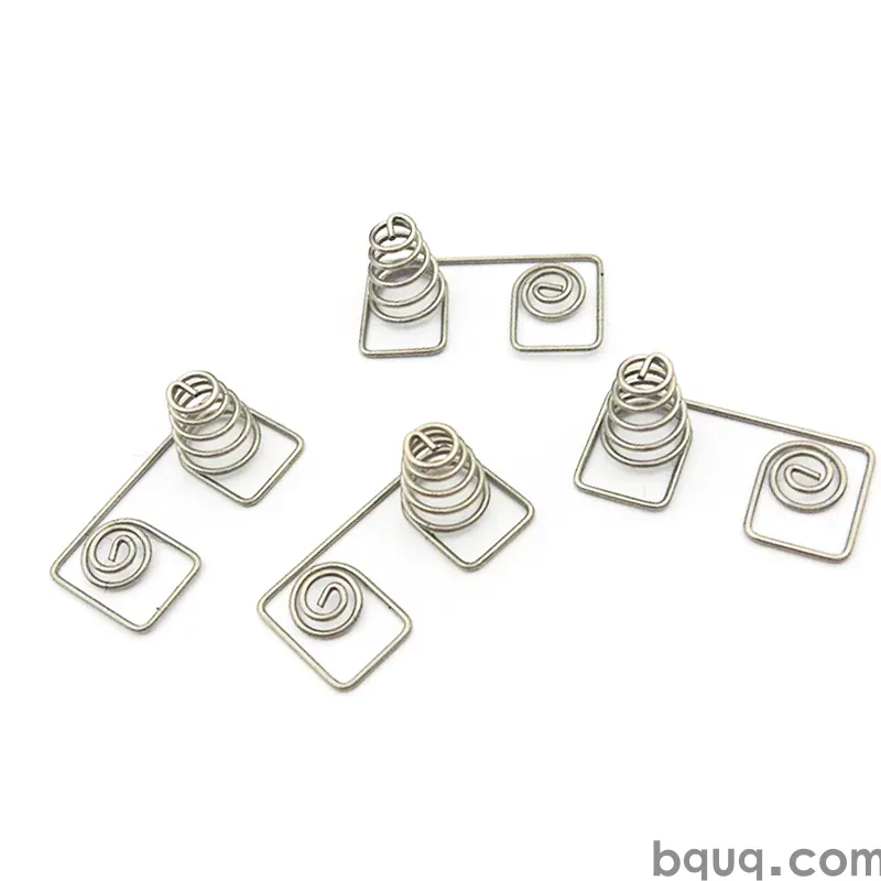
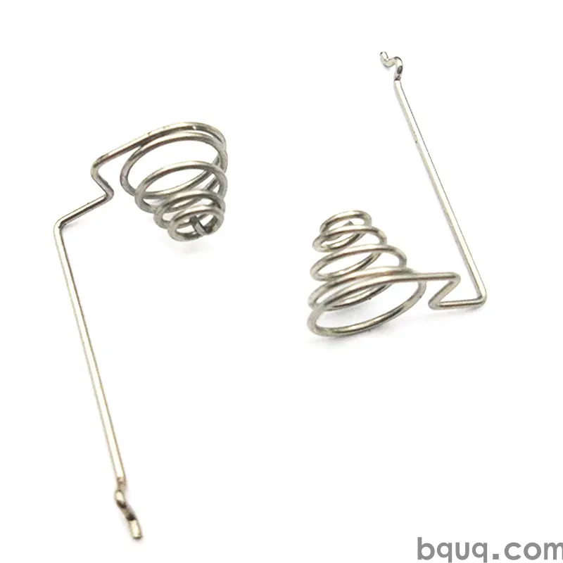
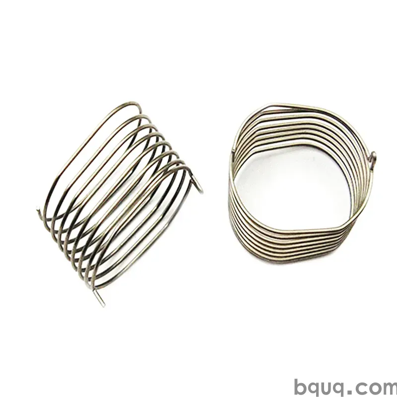
BQUQ runs four production lines in one Dongguan factory covering CNC machining, metal stamping, custom springs, and heat sink production, which means a semiconductor equipment project that needs a machined manifold plus a stamped bracket plus a thermal component can be sourced from one supplier instead of three. That reduces the coordination overhead that usually eats the schedule on multi-part assemblies.
| Stage | What is checked | Typical deliverable |
|---|---|---|
| First article | All drawing dimensions, flatness, finish | FAIR with CMM data |
| In-process | Critical features after each setup | Inspection log |
| Final | Full dimensional and visual check | Final inspection report |
| Pre-ship | Cleanliness, packaging, quantity | Packing list, photos |
For buyers comparing sources, the useful questions are not about the machine list but about process control: how are setups verified, how is flatness measured, what happens when a part is out of tolerance, and who signs the inspection report. Ask for a sample part with a full dimensional report before committing to a production order.
FAQ: sourcing machined semiconductor components
Q: Can a general CNC shop machine semiconductor equipment parts, or do I need a specialist?
A: A capable precision shop can machine most semiconductor hardware, because the work is fundamentally tight-tolerance milling and turning. What separates suppliers is process discipline: stress-relief sequencing, temperature-aware inspection, controlled deburring, and clean packaging. Ask for evidence of those four things rather than a specialty label. BQUQ handles these requirements under ISO9001 with documented inspection at each stage.
Q: What flatness can I realistically expect on a 300 mm aluminum plate?
A: On a 300 mm 6061-T6 plate, 0.025 mm total flatness is a comfortable production target, and 0.01 mm is achievable with stress-relieved stock, rough-and-relax sequencing, and light finishing cuts. Anything tighter should be discussed at the quoting stage, because it changes fixturing, inspection time, and cost significantly. Specify the datum face and measurement temperature alongside the value.
Q: Which stainless grade should I choose for a vacuum chamber component?
A: 304 covers most vacuum-side hardware and is the default for general chamber internals. Choose 316L when the part sees chlorides, acidic residues, or aggressive wet chemistry, since the molybdenum content improves pitting resistance. Both machine similarly, though 316L is slightly gummier. For high-temperature or highly corrosive positions, nickel alloys may be required instead.
Q: How do I prevent particles from machined parts contaminating my process?
A: Control three things: edge quality, surface texture, and packaging. Remove all burrs, especially in gas passages and on sealing lands; keep critical surfaces at Ra 0.8 µm or finer so they clean easily; and specify ultrasonic cleaning followed by individual bagging in cleanroom-compatible film. Avoid untreated paper and loose cardboard, which shed fibers onto clean surfaces during transit.
Q: What lead time and MOQ should I expect for machined semiconductor parts?
A: BQUQ quotes in 12 working hours and works with flexible MOQ, including prototype and low-volume production runs, which suits the semiconductor equipment cycle where designs iterate before volume ramps. Typical lead time depends on material and finishing; nickel alloys and electropolished parts take longer than standard aluminum. Confirm finishing and inspection requirements at the quoting stage so the schedule reflects them.
Related Resources
- About BQUQ and our Dongguan factory: /about/
- CNC machining services: /cnc-machining/
- CNC milling parts: /cnc-milling-parts/
- CNC turning parts: /cnc-turning-parts/
- Industry trends: /industry-dynamics/
- Technical articles: /bquq-blog/
- FAQ and case studies: /faq/ | /case/
- Contact the engineering team: /contact/
Authored by the BQUQ Engineering Team. BQUQ (Dongguan) runs CNC machining (±0.005 mm), metal stamping, custom springs, and heat sink production in one ISO9001 factory. Source-direct from Dongguan, China — quote in 12 hours: sc@bquq.com | WhatsApp +86 13713157787 | www.bquq.com