Thermal Vias and PCB Heat Spreading for SMD Parts
Short answer: A practical SMD thermal stack uses a 2 x 2 to 4 x 4 array of 0.3 mm plated vias under the thermal pad, on 1.0-1.2 mm pitch, tied to at least 2-4 copper layers with 1 oz (35 µm) or 2 oz (70 µm) copper. That gets you roughly 20-40 K/W per via pair in still air, so twenty vias land near 1-3 K/W total. The PCB then feeds a heat sink bonded with a 0.1-0.3 mm interface layer. BQUQ machines and stamps the aluminium or copper heat sink that receives that heat, and quotes in 12 working hours.
Most SMD thermal problems are not solved at the component. They are solved in the 3 mm of material directly beneath it. A QFN, a power MOSFET in a DFN package, or a high-brightness LED all dump heat into a solder pad that is often smaller than 5 mm x 5 mm. That pad has nowhere to go unless the PCB is designed as a heat spreader first and a wiring substrate second.
This article covers the thermal path from die to ambient: via geometry, copper spreading, interface selection, and how the mechanical heat sink is specified so the electrical and thermal design actually connect.
Why does heat spreading matter more than raw heat sink size?
Because the bottleneck is almost never the fin area. It is the constriction resistance between a small die and a large heat sink.
Consider a 5 mm x 5 mm power package dissipating 3 W. If that heat enters a 100 mm x 100 mm heat sink through a 25 mm² contact patch, the spreading resistance inside the base plate dominates. The heat sink may be rated at 1.5 °C/W in free convection, but the effective system resistance can be 8-12 °C/W because the heat never spreads laterally before it reaches the fins.
The fix is a layered approach:
1. Component to pad — solder voiding below 10% by area, verified by X-ray.
2. Pad to inner copper — thermal vias, not just a single connection.
3. Inner copper to board surface — copper pours on every available layer, stitched together.
4. Board to heat sink — a controlled-thickness interface, either a thermal pad, adhesive, or a machined pedestal.
5. Heat sink to air — fin geometry matched to the airflow regime.
Steps 2 and 3 are the ones engineers most often under-build, because they are invisible on the schematic.
How many thermal vias do you actually need?
There is no universal number, but there is a defensible starting range. Via thermal resistance depends on barrel plating thickness, drill diameter, board thickness, and whether the via is filled or open.
The table below gives indicative values for a 1.6 mm FR-4 board with 25 µm copper plating in the barrel. Treat these as design guidance, not datasheet figures.
| Via configuration | Approx. resistance per via | 16-via array (parallel) | Notes |
|---|---|---|---|
| 0.2 mm drill, open barrel | 55-75 K/W | 3.4-4.7 K/W | Highest resistance, cheapest |
| 0.3 mm drill, open barrel | 35-50 K/W | 2.2-3.1 K/W | Common default |
| 0.3 mm drill, filled + capped | 25-35 K/W | 1.6-2.2 K/W | Better for paste printing |
| 0.5 mm drill, open barrel | 20-30 K/W | 1.3-1.9 K/W | Wastes pad area |
| 0.3 mm, 2 oz plating | 18-26 K/W | 1.1-1.6 K/W | Best practical option |
A few practical rules that hold up across most designs:
- 0.3 mm drill on 1.0-1.2 mm pitch is the workhorse. It balances resistance, paste stencil integrity, and manufacturability.
- Stay inside the thermal pad. Vias placed outside the pad footprint do not reduce the constriction resistance at the die.
- Tent or fill the top side. Open vias wick solder paste during reflow and create voids. If you cannot afford filled-and-capped vias, tent the top and leave the bottom open for outgassing.
- More than about 25 vias under a 5 mm pad yields diminishing returns; you are then limited by copper spreading, not via count.
The stacking effect
Vias only help if they land on copper on the other side. A via that terminates on an inner layer with a 2 mm² island is nearly useless. Each via should connect to a plane or a pour with at least 100 mm² of continuous copper, ideally on two or more layers, stitched with additional vias around the perimeter of the pour.
How thick should the copper be?
Copper thickness sets lateral spreading resistance. A 1 oz layer spreads heat noticeably better than 0.5 oz, and 2 oz is a step change again for high-power boards.
| Copper weight | Thickness | Typical use | Spreading benefit |
|---|---|---|---|
| 0.5 oz | 17 µm | Signal-dominant boards | Poor for >1 W |
| 1 oz | 35 µm | Standard power boards | Adequate to ~2-3 W per device |
| 2 oz | 70 µm | LED arrays, motor drivers | Good to ~5 W per device |
| 3 oz+ | 105 µm+ | IGBT, dense LED | Requires wider trace/space rules |
For a typical 1 W SMD part, a 1 oz board with a 400-600 mm² copper pour under and around the device is usually sufficient to keep the junction within limits at 25 °C ambient. For 3 W and above, move to 2 oz or add a metal-core or aluminium-backed substrate.
One caveat: thick copper changes your etch capability. At 2 oz and above, minimum trace width and gap typically widen, which affects routing density. Plan the stack-up before layout, not after.
How do you connect the PCB to a heat sink?
This is where thermal design becomes a mechanical problem, and where a lot of projects lose their gains. A perfect via array feeding a poorly bonded heat sink is a wasted effort.
There are three common attachment routes:
Thermal interface pad or gap filler
A pre-cut pad, typically 0.5-2.0 mm thick, with thermal conductivity in the 1-6 W/m·K range for silicone gap fillers and higher for specialty materials. It accommodates tolerances, is reworkable, and requires no curing. The trade-off is a relatively high interface resistance, often 1-3 °C/W for a 25 mm x 25 mm area at modest pressure.
Choosing the right material is its own exercise — we cover the trade-offs in our guide to thermal interface selection.
Thermal adhesive
Adhesives can reach 1-3 W/m·K and give a thinner bond line, often 0.1-0.2 mm. They are permanent, which matters for rework. If your product needs field repair, plan for it — see heat sink rework and repair.
Machined pedestal contact
The most thermally efficient option is a heat sink with a machined pedestal that contacts the PCB directly, with a thin interface layer only at the pedestal face. This lets you control flatness and height precisely. BQUQ machines these pedestals on CNC-machined heat sinks to ±0.005 mm on critical dimensions, which keeps the bond line uniform across the pad.
A uniform bond line is worth more than a marginally better interface material. A 0.1 mm bond line that varies from 0.05 mm to 0.4 mm across a 25 mm pad creates a hot spot at the thin end and a resistive region at the thick end.
What heat sink geometry suits a via-fed SMD board?
Once heat reaches the heat sink base, the design problem shifts to fin geometry and airflow. Two parameters dominate:
- Fin spacing — too tight and boundary layers merge, killing convection. Too wide and you waste volume. For natural convection, 6-10 mm gaps are typical; for forced air, 2-4 mm. We cover the calculation in detail in natural convection fin spacing.
- Base thickness — must be thick enough to spread heat laterally before it reaches the fins. For a 25 mm x 25 mm heat source on a 100 mm heat sink, a 5-8 mm base is a reasonable starting point. Thinner bases save weight but reintroduce constriction resistance.
For SMD boards with a single dominant heat source, an extruded profile with a thick base and moderate fin count usually beats a large, thin-based heat sink. For distributed sources — LED arrays, multi-rail power stages — a flatter base with denser fins and forced air is more effective.
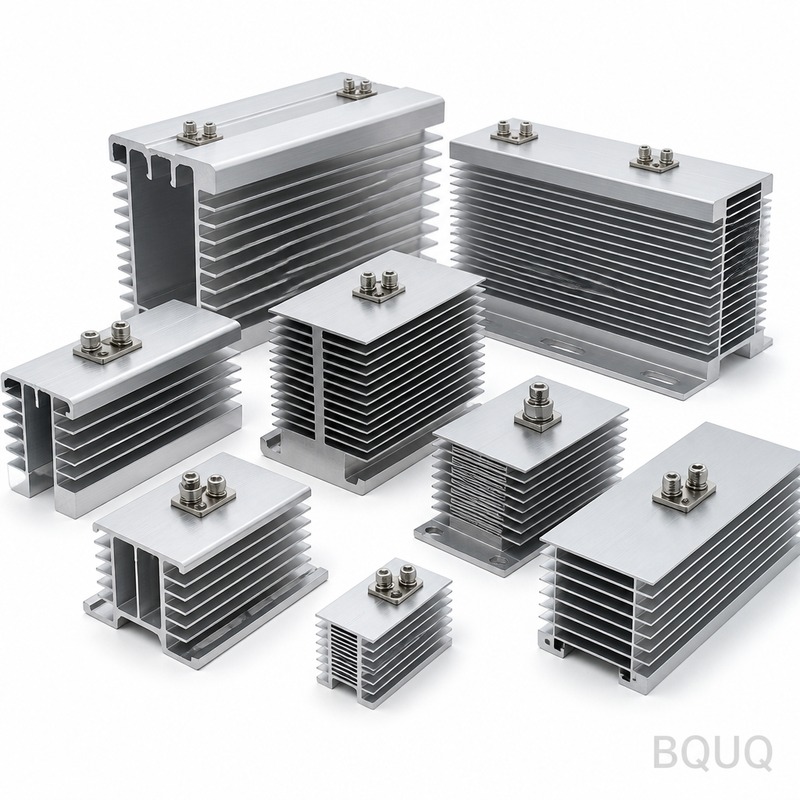
BQUQ produces heat sinks across all these formats: extruded profiles, stamped and bonded assemblies, skived fin, die-cast, and CNC-machined variants with machined pedestals and mounting features. The full range is listed under heat sinks, and pedestal-critical parts are covered under CNC-machined heat sinks.
Design checklist for a via-fed SMD thermal stack
| Step | Target | Common failure |
|---|---|---|
| Solder voiding under pad | <10% area | Paste volume too low, open vias wicking |
| Via count and pitch | 16-25 vias, 0.3 mm, 1.0-1.2 mm pitch | Vias placed outside pad |
| Via termination | Plane on 2+ layers | Via lands on isolated island |
| Copper weight | 1 oz min, 2 oz for >3 W | 0.5 oz on a 2 W part |
| Copper pour area | 400-600 mm² per watt-class | Pour clipped by routing |
| Interface layer | 0.1-0.3 mm, uniform | Uneven pedestal, thick pad |
| Heat sink base | 5-8 mm for 25 mm source | Thin base, high constriction |
| Fin spacing | Matched to airflow mode | Natural-convection spacing in a fan duct |
Frequently Asked Questions
Q: Can I use thermal vias under a QFN without filling them?
A: Yes, but tent the top side with solder mask and leave the bottom open. Open vias act as paste wicking paths during reflow, which pulls solder away from the thermal pad and creates voids. If your stencil aperture and paste volume are tightly controlled, open vias are workable for low-volume builds. For anything above a few thousand units, filled and capped vias give more repeatable results and better thermal performance.
Q: How much does a copper pour actually help compared to just using more vias?
A: It usually helps more. Vias move heat vertically; copper moves it laterally. A dense via array terminating on a small island still concentrates heat. A 500 mm² pour on two layers, stitched with perimeter vias, spreads heat across the board and lowers the effective source-to-sink resistance far more than doubling the via count under the pad. Build both, but do not neglect the pour.
Q: What is the minimum practical heat sink base thickness for an SMD board?
A: For a 25 mm x 25 mm heat source, 5 mm is a reasonable floor and 6-8 mm is safer for sources above 3 W. Below 4 mm, constriction resistance inside the base starts to dominate and adding fin area stops helping. If weight is critical, a copper spreader plate bonded into an aluminium heat sink base gives better spreading per gram than simply thickening the aluminium.
Q: Does via plating thickness matter as much as via diameter?
A: It matters a lot at small diameters. A 0.3 mm via with 25 µm barrel plating has roughly 35-50 K/W; the same via with 50 µm plating drops to about 18-26 K/W. Since barrel plating thickness is set by your board house's process, specify it explicitly on the fabrication drawing. If you cannot control it, use more vias rather than relying on plating thickness.
Q: How do I know whether my thermal stack is adequate before building hardware?
A: Run a thermal simulation with the via array, copper weight, and pour area modelled explicitly — lumped models hide constriction resistance. Then validate with a thermal test board that includes the actual heat sink and interface material. Measure the case temperature and the heat sink base temperature separately; the difference tells you whether the interface or the heat sink is your bottleneck. Adjust the cheaper one first.
Related Resources
- About BQUQ and our Dongguan production lines: /about/
- Full heat sink product range: /heat-sinks/
- Extruded heat sink profiles: /extruded-heat-sinks/
- Industry trends in thermal management: /industry-dynamics/
- Technical articles library: /bquq-blog/
- Frequently asked questions: /faq/
- Case studies: /case/
- Contact the engineering team: /contact/
Authored by the BQUQ Engineering Team. BQUQ (Dongguan) runs CNC machining (±0.005 mm), metal stamping, custom springs, and heat sink production in one ISO9001 factory. Source-direct from Dongguan, China — quote in 12 hours: sc@bquq.com | WhatsApp +86 13713157787 | www.bquq.com