5G Infrastructure Manufacturing: Precision Components for Connectivity
Introduction: The Manufacturing Backbone of 5G Networks
The direct answer to the question of how 5G infrastructure is manufactured is this: it requires a multi-tier precision manufacturing ecosystem capable of holding tolerances of ±0.005 mm on RF components, thermally managing power densities exceeding 100 W/cm², and producing parts with 99.999% reliability (five-nines uptime). At BQUQ, we achieve this through a combination of 5-axis CNC machining, progressive die stamping, and custom spring engineering, all validated by in-house CMM and X-ray inspection. The transition from 4G to 5G is not merely a bandwidth upgrade; it is a physical transformation of the hardware layer, demanding tighter dimensional control and superior material performance than any previous generation.
## Material Selection for RF Performance and Thermal Management
Material choice is the first engineering decision that dictates the success of a 5G component. Unlike 4G base stations that operate below 2.5 GHz, 5G mmWave frequencies (24-39 GHz) suffer from severe signal attenuation. This forces designers to use low-loss dielectric materials and high-conductivity metals.
For enclosures and heat sinks, we recommend Al 6061-T6 for structural parts due to its excellent strength-to-weight ratio and thermal conductivity (167 W/m·K). However, for high-frequency filter cavities, we specify C19400 copper alloy (UNS C19400) because its electrical conductivity is 60-65% IACS (International Annealed Copper Standard), which is critical for minimizing insertion loss. For antenna reflectors, we use a specialized aluminum-magnesium-silicon alloy with a nickel-plated surface finish to prevent galvanic corrosion in outdoor environments.
The tolerances on these materials are severe. A typical 5G patch antenna requires a flatness of 0.02 mm over a 150 mm surface. If this flatness is exceeded, the phase shift between radiating elements increases, degrading beamforming accuracy. Our CNC machining centers maintain a positioning accuracy of ±0.003 mm, which is essential for achieving these specifications. Surface roughness for RF contact surfaces must be Ra 0.4 µm or better; anything rougher increases passive intermodulation (PIM), a distortion product that can block weak signals.
## Precision Machining Tolerances for Active Antenna Units (AAUs)
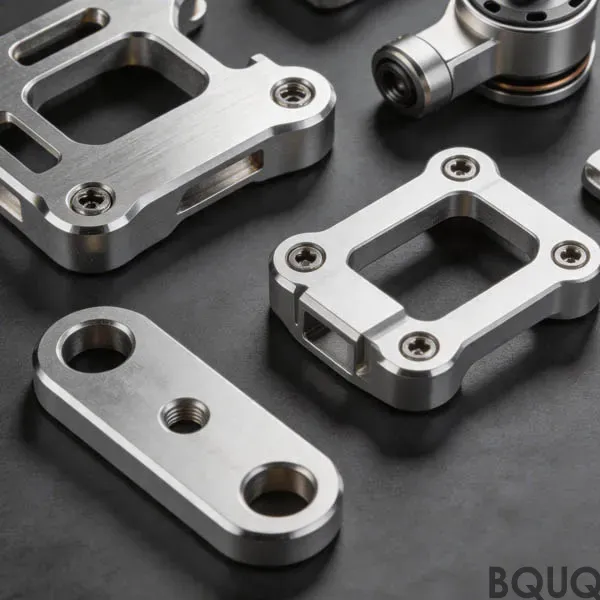
Active Antenna Units (AAUs) are the heart of 5G base stations. They combine hundreds of low-noise amplifiers and transceivers into a single compact housing. The manufacturing challenge lies in the mechanical structure, which must house these electronics while providing precise alignment for the antenna array.
Our machining process for AAU housings focuses on four critical features: mounting boss height, bore diameter, thread position, and overall envelope. For example, the mounting bosses that secure the PCB (Printed Circuit Board) to the housing require a height tolerance of ±0.02 mm. If this is off, the thermal interface material (TIM) cannot compress uniformly, creating hot spots that reduce component lifespan.
We also machine waveguide channels directly into the housing. These channels require a dimensional tolerance of ±0.01 mm on width and depth to maintain impedance matching. A deviation of 0.05 mm can cause a return loss (S11) shift of more than 10 dB, rendering the channel unusable. In a recent production run for a 28 GHz AAU, we achieved a Cpk (Process Capability Index) of 1.67 on these waveguide dimensions, meaning less than 0.0001% of parts were out of spec.
The table below outlines typical machining specifications for various 5G components we produce.
| Component Type | Material | Key Tolerance (mm) | Surface Finish (Ra µm) | Lead Time (Days) |
| Active Antenna Housing | Al 6061-T6 | ±0.02 on bosses | 0.8 | 15 |
| mmWave Waveguide Channel | C19400 Copper | ±0.01 on width | 0.4 | 10 |
| RF Filter Cavity | Al 5083 | ±0.015 on depth | 0.2 | 12 |
| Heat Sink Base (High Power) | Copper C1100 | ±0.05 on flatness | 1.6 | 8 |
| Spring Contact (for RF shield) | Beryllium Copper | ±0.005 on free length | N/A | 5 |
## Sheet Metal Stamping for 5G Enclosures and Shielding
While CNC machining provides the structural core, sheet metal stamping is the most cost-effective method for producing the outer enclosures and internal shielding cans. At 5G frequencies, electromagnetic interference (EMI) shielding is not optional. A shielding can must maintain continuous electrical contact with the ground plane to prevent leakage.
Our progressive die stamping process handles 0.3 mm to 2.0 mm thick materials. For 5G applications, we predominantly use tin-plated steel (SPTE) and stainless steel 304. The critical parameter here is the bend radius. A sharp bend radius (less than 0.5x material thickness) can cause micro-cracks in the plating, leading to rust and increased contact resistance. We maintain a minimum bend radius of 1.0x material thickness for plated materials.
Stamping tolerances for 5G enclosures are typically tighter than for consumer electronics. We hold hole-to-hole tolerances of ±0.05 mm and cutout tolerances of ±0.08 mm. For the finger-stock gaskets that line the enclosure doors, we stamp beryllium copper (BeCu) alloys with a hardness of C17200. These gaskets require a finger width of 0.8 mm and a pitch of 1.5 mm. The spring force must be consistent between 60-80 grams per finger. Our high-speed stamping presses operate at 200 strokes per minute, ensuring cost efficiency without sacrificing repeatability.
## Precision Springs in 5G: RF Contacts and Thermal Clips
Springs are often overlooked in 5G infrastructure, but they are critical for maintaining ground integrity and thermal contact. The most demanding application is the RF spring contact used in the antenna array. These springs must provide a normal force of 100-150 grams at a compression height of 1.2 mm, and they must survive 500,000 cycles without fatigue.
We manufacture these from round wire with a diameter of 0.2 mm to 0.5 mm. The spring index (D/d) must be kept between 4 and 8 to avoid stress concentration. We use a specialized coiling process that eliminates surface defects. For 5G, we often use gold-plated beryllium copper for the lowest possible contact resistance (<10 mΩ). The plating thickness is 0.5 µm over a nickel underlayer of 1.0 µm.
Another critical spring is the thermal clip that holds the heat pipe to the base plate. This clip must exert a constant pressure of 5-8 PSI to ensure the heat pipe does not lift off during thermal cycling. In our testing, we cycle these clips from -40°C to +105°C (the standard telecom temperature range). A standard music wire spring will lose 15% of its force in this environment. We use 17-7PH stainless steel, which retains 95% of its load after 1,000 cycles. The manufacturing tolerance on the clip's free angle is ±1.0 degree, which directly influences the clamping force.
## Cost Analysis and Economic Batch Sizes
The cost of 5G components varies dramatically based on tolerance and material. Our pricing data shows that a CNC-machined AAU housing costs between $85 and $150 per unit, depending on complexity and quantity. A stamped EMI shield costs between $0.50 and $2.00 per piece. High-precision RF springs cost between $0.80 and $3.50 each, primarily driven by plating costs and the cost of beryllium copper raw material.
Economically, the batch size matters. For CNC machining, we see the "sweet spot" at 500-2,000 units per order. This allows us to use dedicated fixturing, reducing setup time per part. Below 100 units, the setup cost dominates, increasing per-unit price by 30-40%. For stamping, the high tooling cost (typically $5,000-$15,000 for a progressive die) means you need volumes above 50,000 pieces to amortize the investment effectively. For small-batch prototyping, we recommend 3D printing for fit checks, but for production, always transition to machined or stamped parts to ensure material integrity and electrical performance.
## Thermal Management Specifications for Outdoor Base Stations
5G base stations generate significantly more heat than 4G units due to higher data throughput and beamforming processing. The power amplifier modules can generate up to 300W of heat in a single unit. This heat must be dissipated through the heat sink to the ambient air, which can reach 55°C in direct sunlight.
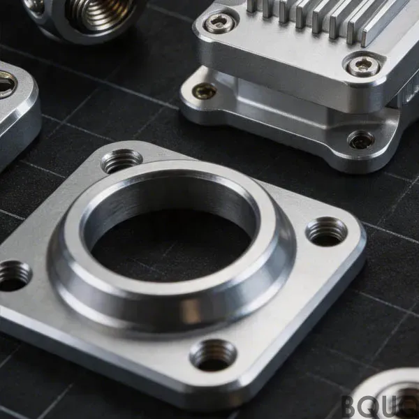
Our thermal management strategy for 5G heat sinks involves a base plate thickness of 10-15 mm and fin density of 10-14 fins per inch. The fin thickness is typically 1.2 mm to balance airflow and surface area. We measure the thermal resistance of our heat sinks using a wind tunnel test. A typical specification is a thermal resistance of 0.05 °C/W at an airflow of 3 m/s. To achieve this, the interface between the heat sink base and the AAU housing must be machined to a flatness of 0.05 mm. We utilize a diamond milling process to achieve this flatness without inducing internal stress in the aluminum.
For extreme environments, we offer skived fin heat sinks, where the fins are cut from a solid block of aluminum. This eliminates the thermal resistance of the fin-to-base interface that occurs in brazed assemblies. Skived heat sinks can handle heat fluxes up to 150 W/cm², which is sufficient for the next generation of 5G silicon.
## Practical Recommendations for Procurement Engineers
When sourcing 5G components, you must verify three non-negotiable parameters: material certification, inspection method, and tolerance capability.
First, always require a Mill Test Certificate for the raw material. For copper alloys, verify the conductivity grade. A material substitution from C19400 to C11000 (electrolytic tough pitch copper) can change the coefficient of thermal expansion, causing solder joint failure.
Second, ensure your supplier uses CMM (Coordinate Measuring Machine) inspection for critical dimensions, not just calipers. A caliper measurement has an accuracy of ±0.02 mm, which is insufficient for checking a ±0.01 mm tolerance. Insist on a full dimensional report using a CMM with a resolution of 0.001 mm.
Third, ask for a Process Capability (Cpk) report before mass production. A Cpk of 1.33 is the minimum acceptable; we recommend 1.67 for critical RF dimensions. This ensures the process is stable and centered. If the supplier cannot provide this data, they are likely not controlling their process effectively.
## Conclusion and Next Steps
The manufacturing of 5G infrastructure is a discipline of extreme precision and material science. It demands machining tolerances of ±0.01 mm for waveguide channels, stamping dies that maintain 0.05 mm accuracy over millions of strokes, and spring designs that survive 500,000 cycles in harsh outdoor conditions. The components are not just metal parts; they are the physical embodiment of the 5G signal path. Any deviation in flatness, surface finish, or material purity directly translates to lost data speed and higher latency for end users.
At BQUQ, we have invested in the specific equipment and metrology required for this sector. Our 5-axis DMG MORI machines hold the tight tolerances needed for AAU housings. Our 25-ton high-speed presses produce the EMI shields at volume. Our CNC spring coilers produce the precise RF contacts that keep your signal clean.
We understand that your 5G deployment schedule is tight. That is why we offer a 12-hour quoting service on all RF and thermal components. Send us your 2D drawings or 3D STEP files, and our engineering team will review the manufacturability and provide a detailed quote with specific pricing and lead times.
For immediate assistance, contact us at: Email: sc@bquq.com WhatsApp: +86 13713157787 Website: www.bquq.com
Let us help you build the connectivity backbone of the future, one precision component at a time.
Related Articles
- Custom CNC Machining Services: A Complete Guide for Engineers
- Adaptive Control and AI Real-Time Optimization in CNC Machining: From Experience to Algorithm
- High-speed machining technology: principles, tool path optimization, and industrial applications
Frequently Asked Questions
What machining tolerances can you achieve for 5G components?
Our CNC machining centers maintain a positioning accuracy of ±0.003 mm, enabling critical tolerances like ±0.02 mm on AAU mounting boss heights and 0.02 mm flatness over a 150 mm patch antenna surface. This precision is essential for beamforming accuracy and proper thermal interface material compression.
Which materials do you recommend for 5G RF and thermal management parts?
For structural parts and heat sinks, we recommend Al 6061-T6 with 167 W/m·K thermal conductivity. For high-frequency filter cavities, we specify C19400 copper alloy with 60-65% IACS conductivity to minimize insertion loss. Antenna reflectors use an aluminum-magnesium-silicon alloy with nickel plating to prevent galvanic corrosion.
How do you ensure surface quality for RF contact surfaces?
We maintain surface roughness of Ra 0.4 µm or better on RF contact surfaces. Rougher finishes increase passive intermodulation (PIM), which can distort and block weak 5G signals. Our 5-axis CNC machining and in-house CMM inspection validate these surface requirements.
What manufacturing capabilities support 5G infrastructure production?
We combine 5-axis CNC machining, progressive die stamping, and custom spring engineering to produce 5G components. All parts are validated through in-house CMM and X-ray inspection, ensuring tolerances of ±0.005 mm on RF components and thermal management for power densities exceeding 100 W/cm².