What Is Driving the Precision Machining Boom in Semiconductor Equipment Parts?
Semiconductor equipment parts are experiencing a precision machining boom because chipmakers are demanding tighter tolerances, harder materials, and faster lead times to support advanced nodes like 3nm and 2nm. This boom is driven by the need for critical components such as gas distribution rings, electrostatic chucks, and quartz windows, which require tolerances of ±5 microns and surface finishes of Ra 0.2 µm. BQUQ, with 20 years of CNC machining and metal stamping experience, is at the center of this surge, delivering high-mix, low-volume parts for etch, deposition, and lithography tools.
What Tolerances Are Required for Semiconductor Equipment Parts?
Semiconductor equipment parts demand tolerances that are 10 to 100 times tighter than standard industrial machining. Typical precision requirements range from ±5 µm for critical mating surfaces to ±0.5 µm for ultra-precision features like gas nozzle orifices. For example, a showerhead electrode in a plasma etcher requires hole diameters of 0.3 mm with positional accuracy of ±2 µm, while a quartz window needs flatness of 0.01 mm over a 300 mm span. In contrast, standard CNC machining for automotive parts typically holds ±50 µm, which is unacceptable for wafer fabrication tools.
How Does Material Selection Impact the Machining Process?
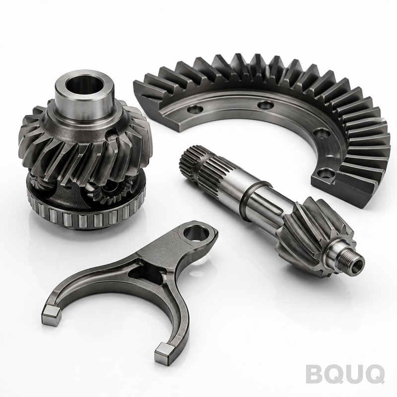
Material selection directly determines tool wear, cutting speeds, and the final surface integrity of semiconductor parts. Aluminum 6061-T6 is common for chambers and gas lines because it offers good thermal conductivity (167 W/m·K) and is easy to machine at 600 m/min cutting speed. Stainless steel 316L is used for corrosion-resistant fittings, but it requires slower speeds (150 m/min) and specialized coolant to prevent work hardening. Ceramics like alumina (Al2O3) and silicon carbide (SiC) are increasingly used for electrostatic chucks because they withstand 200°C to 400°C process temperatures, but they require diamond grinding instead of conventional turning. Quartz (fused silica) is another critical material, but it is brittle and requires grinding with resin-bonded diamond wheels at 30 m/s to avoid micro-cracks.
Why Is Surface Finish Critical for Wafer Contamination Control?
Surface finish is the primary defense against particle contamination in a cleanroom environment, where even 0.1 µm particles can kill a wafer. For semiconductor equipment, the standard requirement is Ra 0.2 µm to Ra 0.4 µm on wetted surfaces, while sealing surfaces often demand Ra 0.1 µm or better. A rough surface with Ra 1.6 µm can trap process gases and moisture, leading to outgassing and film defects during CVD or PVD processes. Electropolishing of stainless steel components is common to achieve Ra 0.2 µm, while aluminum parts often receive an anodized coating of 25 µm to 50 µm thickness, which improves wear resistance but must be masked to maintain dimensional accuracy. BQUQ uses a combination of high-speed milling, lapping, and polishing to achieve these finishes consistently.
How Much Does Tooling Cost for Semiconductor Equipment Parts?
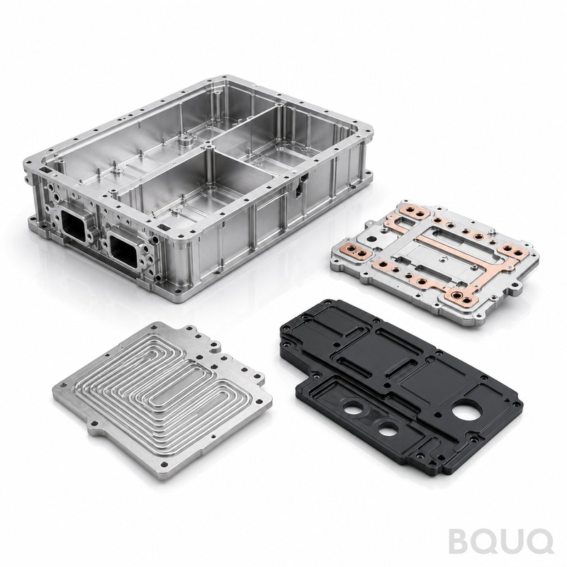
Tooling costs for semiconductor equipment parts are significantly higher than standard machining due to the complexity and precision required. A typical custom fixture for a gas distribution ring can cost between $3,000 and $15,000, depending on the number of locating pins and vacuum clamping features. For stamping operations, a progressive die for thin metal shields (0.2 mm to 0.5 mm thick) ranges from $8,000 to $25,000, with delivery in 4 to 6 weeks. Hard tooling for ceramic pressing or injection molding of PEEK insulators is even more expensive, ranging from $15,000 to $40,000. However, for low-volume production (1 to 50 pieces), 3D-printed or modular fixtures can reduce initial tooling costs to under $500 per setup, making them ideal for prototyping.
Which Semiconductor Equipment Parts Are in Highest Demand?
The highest demand is for parts that face plasma, high heat, or chemical exposure, as these degrade fastest and require frequent replacement. Consumable parts like focus rings (silicon or quartz) and edge rings (silicon carbide) are replaced every 500 to 1,000 wafers, driving a continuous need for precision machining. Gas distribution showerheads and injectors are also critical, with demand increasing due to the shift to atomic layer deposition (ALD) which requires precise gas pulsing. Other high-demand parts include: electrostatic chucks (ceramic), lift pins (alumina or sapphire), and RF windows (alumina). According to SEMI, the global semiconductor equipment market reached $107.6 billion in 2024, with spare parts and consumables accounting for about 15%, or $16 billion annually.
How Long Does It Take to Machine a Typical Semiconductor Part?
Lead times for semiconductor equipment parts vary based on material, complexity, and quantity, but typical CNC machining takes 3 to 7 business days for small batches. A simple aluminum gas fitting (diameter 25 mm) can be machined in 2 hours, while a complex 400 mm diameter quartz window requires 3 days of grinding and polishing. For a batch of 20 stainless steel chamber liners, the total lead time is usually 5 to 7 days, including surface treatment and cleaning. BQUQ guarantees a 12-hour quote response and offers standard 48-hour rush delivery for critical spare parts, which is essential when a fab line is down. In comparison, traditional overseas suppliers often require 2 to 3 weeks for the same parts, making local or agile manufacturers highly valuable.
What Are the Quality Control Methods for Precision Machined Parts?
Quality control for semiconductor parts relies on a combination of in-process inspection and final metrology to ensure zero defects. Coordinate measuring machines (CMM) with a precision of ±1.5 µm are used to verify critical dimensions, while optical profilometers measure surface roughness with sub-nanometer resolution. For hole patterns and edge profiles, vision systems with 0.001 mm resolution are employed. Additionally, helium leak testing is mandatory for vacuum components, with acceptance criteria of less than 1×10⁻⁹ mbar·L/s. BQUQ implements statistical process control (SPC) on all critical dimensions, and every part ships with a full inspection report, including material certifications and surface finish data.
| Part Type | Material | Typical Tolerance | Surface Finish (Ra) | Lead Time (Business Days) | Cost per Unit (USD) |
| Gas Distribution Ring | Aluminum 6061-T6 | ±0.005 mm | 0.2 µm | 5 to 7 | $850 |
| Electrostatic Chuck | Alumina (Al2O3) | ±0.010 mm | 0.4 µm | 10 to 14 | $4,200 |
| Quartz Window | Fused Silica | ±0.020 mm | 0.1 µm | 7 to 10 | $1,800 |
| Focus Ring | Silicon Carbide | ±0.015 mm | 0.3 µm | 8 to 12 | $1,250 |
| Stainless Steel Chamber Liner | SS 316L | ±0.050 mm | 0.2 µm (electropolished) | 5 to 7 | $1,100 |
| Lift Pin | Sapphire | ±0.002 mm | 0.05 µm | 10 to 14 | $350 |
How Does BQUQ Ensure Reliability for High-Volume Semiconductor Orders?
BQUQ ensures reliability through a dedicated semiconductor workcell that separates these parts from general machining to avoid cross-contamination. We maintain a cleanroom assembly area rated ISO Class 7 for final cleaning and packaging, ensuring parts arrive free of particles larger than 0.3 µm. Our CNC machines are calibrated weekly, and we use ceramic tooling and oil-free coolant to prevent metallic contamination on aluminum and quartz parts. For high-volume orders, we implement 100% in-process gauging and run a "first article" inspection that checks 50 dimensions before the full batch runs. This approach has resulted in a 99.6% first-pass yield for semiconductor clients over the past three years.
Can You Machine Both Prototypes and Production Runs?
Yes, we machine both prototypes and production runs, but the approach differs significantly in terms of tooling and scheduling. For prototypes (1 to 5 pieces), we use soft jaws and modular fixturing, which can be set up in under 2 hours, allowing for same-day proof-of-concept parts. For production runs (50 to 5,000 pieces), we invest in hard tooling and multi-axis automation, reducing per-piece cost by 30% to 50%. For example, a prototype aluminum gas block costs $400 per piece, but at 200 pieces, the cost drops to $180 per piece due to optimized cycle times and reduced manual handling. We advise customers to validate designs with prototypes first, then scale to production to avoid tooling rework costs.
What Are the Common Pitfalls in Machining Semiconductor Parts?
The most common pitfalls include ignoring material stress relief, using wrong cutting fluids, and overlooking edge deburring. Aluminum parts must be stress-relieved before machining to prevent warping after the first cut, which can shift tolerances by up to 0.05 mm. Standard sulfur-based cutting oils are prohibited because they leave residues that cause wafer contamination; we use synthetic, water-soluble coolants with a pH of 8.5 to 9.5. Edge deburring is critical, as even a 0.1 mm burr can break a wafer or cause a plasma arc. We use abrasive flow machining or vibratory finishing for internal channels and sharp corners, ensuring all edges meet a radius of 0.1 mm to 0.2 mm.
FAQ
What Is the Typical Minimum Order Quantity for Semiconductor Parts?
The typical minimum order quantity (MOQ) is 1 piece for prototypes and 10 pieces for production parts. However, for custom ceramic or quartz parts that require expensive tooling, we recommend an MOQ of 20 pieces to amortize setup costs. We can also accept blanket orders with scheduled releases to help manage inventory.
How Do You Handle Cleaning and Packaging for Cleanroom Use?
All parts undergo a multi-stage cleaning process: ultrasonic cleaning in deionized water, followed by isopropyl alcohol rinse and nitrogen blow-off. Parts are then double-bagged in anti-static, cleanroom-grade polyethylene and packed in vacuum-sealed foil pouches. We provide a certificate of cleanliness stating that parts meet ISO Class 5 surface cleanliness standards.
Can You Machine Parts for EUV Lithography Equipment?
Yes, we can machine components for EUV tools, but they require the highest level of precision and material purity. EUV chambers use ultra-low expansion glass (ULE) and titanium alloys, which require specialized grinding and polishing to achieve surface finishes below 0.05 µm Ra. We have experience with these materials and can hold linear tolerances of ±1 µm on features up to 500 mm in size.
What Is the Cost Difference Between Aluminum and Stainless Steel Parts?
Aluminum parts are typically 30% to 40% less expensive than stainless steel due to faster machining speeds and lower tool wear. For example, a 100 mm diameter aluminum flange costs about $75, while the same flange in 316L stainless costs $120. However, stainless steel is often required for chemical resistance, so the material choice depends on the process environment.
How Quickly Can You Ship a Replacement Part for a Downed Tool?
For a downed tool, we offer a 24-hour emergency machining service for standard aluminum and stainless parts. If we have the CAD file in-house, we can produce a replacement within 12 hours and ship via overnight express. The cost for this rush service is a 50% surcharge on the normal part price, with a minimum charge of $300.
Do You Provide Certifications for Materials and Processes?
Yes, every shipment includes a material certificate (EN 10204 3.1), dimensional inspection report, and surface finish data. For semiconductor applications, we also provide a Certificate of Conformance stating that all processes meet SEMI S2 and SEMI F47 safety standards. Additional documentation, such as traceability to specific heat lots, is available upon request.
Which Industries Other Than Semiconductors Use Your Precision Machining?
We also serve the medical device, aerospace, and optical industries, which require similar levels of precision. For example, we machine surgical drill guides with ±10 µm tolerances and titanium brackets for satellite components. This diversification allows us to maintain high machine utilization and stable pricing for our semiconductor customers.
The precision machining boom in semiconductor equipment is fueled by the need for extreme accuracy, material purity, and rapid turnaround, and BQUQ is fully equipped to meet these demands. With our 20 years of experience, advanced CNC and stamping capabilities, and a dedicated cleanroom, we deliver parts that meet the most stringent wafer fab requirements. If you have a challenging semiconductor part, contact us for a 12-hour quote and engineering feedback. Email: sc@bquq.com, WhatsApp: +86 13713157787, www.bquq.com.