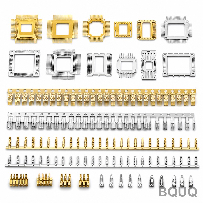
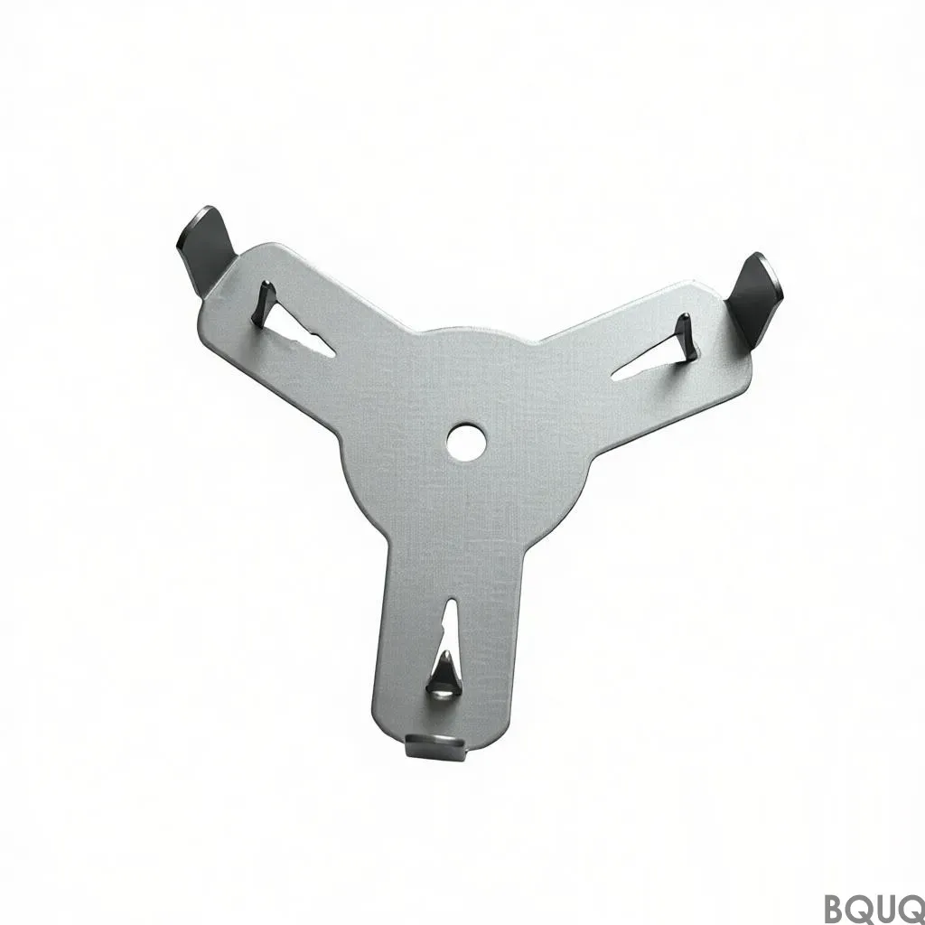
Our Precision Stamped Lead Frames Collection is a family of high-density metal carriers used to support and interconnect semiconductor dies, sensor arrays, and optoelectronic packa
Precision Stamped Lead Frames Collection | BQUQ Precision Manufacturing
Our Precision Stamped Lead Frames Collection is a family of high-density metal carriers used to support and interconnect semiconductor dies, sensor arrays, and optoelectronic packages. We hold flatnes
Get a Fast Quote for This Part
Send us your drawing / quantity / material — reply within 24h.
Our Precision Stamped Lead Frames Collection is a family of high-density metal carriers used to support and interconnect semiconductor dies, sensor arrays, and optoelectronic packages. We hold flatness within 0.02 mm over 50 mm length, stamping tolerance at ±0.01 mm, and surface finish at Ra 0.4 µm, with a standard production lead time of 7 working days. Every frame is made from certified strip stock in our Dongguan factory, so you get the precision of a dedicated toolroom without the import delays.
How We Hold ±0.01 mm Across High-Speed Die Stamping
Our presses run at 200 to 600 strokes per minute, but speed does not dictate accuracy. We use progressive dies with carbide inserts, ground to a mirror finish, and we re-certify die wear after every 50,000 strokes. The strip is guided through servo-driven feed units with closed-loop length control, which eliminates pitch error before it starts. We also run a 100% optical inspection on critical lead tips — not a sample — so you receive frames where every finger sits where the CAD file says it should.
Materials and Heat Treatment That Prevent Lead Fatigue
We stock C19400 (copper-iron), C70250 (copper-nickel-silicon), and Alloy 42 (iron-nickel) in thicknesses from 0.10 mm to 0.50 mm. For high-cycle applications, we specify C19400 in half-hard or full-hard temper, which gives a typical hardness of 120–160 HV. If you need higher strength, we heat-treat Alloy 42 to 180–220 HV after stamping, but we keep the process controlled so that the surface stays free of oxide scale. We do not bend, stress-relieve, or plate without first confirming the strip’s grain direction.
Selective Plating and Solderability We Guarantee
Most lead frames fail at the interface, not the stamping. That is why we offer selective silver plating (2.5–5.0 µm) and nickel-palladium-gold finish (0.5–1.0 µm) only on the bonding areas, leaving the rest of the frame bare to reduce cost. We test solderability per JIS C 0050, using a wetting balance to confirm zero dewetting after steam aging. If you run lead-free reflow, we can pre-verify compatibility with your paste profile — just send the temperature curve.
Dimensional Inspection Before Every Shipment
We do not ship a batch unless the first article and the last article pass the same gate. Our QC lab uses a CNC vision measuring machine with a resolution of 0.5 µm, a profilometer for Ra, and a hardness tester calibrated to ASTM E18. For every order, we issue a dimensional report covering lead width, lead pitch, coplanarity, and burr height. Burr height stays under 5% of material thickness — that is our internal cap, not a customer request.
Packaging and Anti-Static Protection for Die Attach
Frames arrive in anti-static trays or on 13-inch reels, depending on your pick-and-place line. We use anti-tarnish paper between layers and vacuum-seal the reel in moisture-barrier bags with desiccant and humidity indicator cards. If you run automated die attach, we can add a peel-off cover film to prevent dust accumulation. Each box carries a lot number, so you can trace the strip coil, die number, and operator back to the exact shift.
Prototyping to Production Without Tooling Surprises
We build the prototype die in 10 days and ship 50 to 200 pieces for your fit-out test. After you approve the samples, we transfer the same die geometry to a hardened production die — no redesign, no tolerance drift. We keep the prototype tooling on file for 24 months, so your next revision starts from a known baseline. This is how we keep your project moving whether you need 200 pieces or 2 million.
Cost Per Frame vs. Total Cost of Ownership
Cheaper stamping shops often quote a lower per-piece price but add hidden costs: slower delivery, inconsistent plating, and rejected batches that stall your line. Our frames cost 5–10% more per piece on the first order, but we cut scrap rates below 0.3% and ship on time 98% of the time. Add the cost of a stalled SMT line, and our price becomes the cheaper option. For a full comparison of how precision affects your machining budget, see our CNC machining tolerances guide.
Matching the Right Tool to Your Lead Frame Material
Stamping dies are cutting tools, and they wear like any other. If you are designing the mating tooling or fixtures for these frames, the CNC cutting tool selection guide explains how to choose carbide grades and coatings for the same copper alloys we stamp. The guide covers edge life and chip load for C19400, which will help you avoid tool breakage when machining your own test fixtures.
Parameter
Specification / Range
Materials
C19400, C70250, Alloy 42, C15100
Strip thickness
0.10 mm – 0.50 mm
Stamping tolerance
±0.01 mm
Flatness
0.02 mm max over 50 mm length
Hardness (C19400)
120 – 160 HV (half-hard to full-hard)
Hardness (Alloy 42)
180 – 220 HV (after heat treatment)
Surface finish (Ra)
0.4 µm on stamped surfaces
Burr height
≤ 5% of material thickness
Lead time (prototype)
10 working days
Lead time (production)
7 working days after approval
MOQ
No MOQ (1 piece for prototype)
Plating options
Selective Ag (2.5–5.0 µm), NiPdAu (0.5–1.0 µm)
What is the minimum order quantity for this collection?
We have no MOQ — you can order 1 prototype piece or 1 million production frames, and the per-piece price adjusts only with volume.
Can I customize the frame shape and plating pattern?
Yes, we build custom dies for any outline, lead count, and selective plating area — just send a 2D/3D file and your assembly requirements.
How do you ensure quality for a large batch?
We run SPC on critical dimensions every 2 hours, plus a 100% optical check on lead tips and coplanarity before packing.
What is your typical lead time for a stamped lead frame order?
Prototype dies take 10 working days; production orders ship 7 working days after sample approval, with faster options for repeat tools.
We are a precision manufacturing factory in Dongguan, China, with 20 years of CNC machining and stamping experience. Our Precision Stamped Lead Frames Collection is built for engineers who cannot afford dimensional drift. Send your drawing today for a firm quote within 12 hours — email sc@bquq.com or WhatsApp +86 13713157787. We will reply with a DFM review, a cost breakdown, and a delivery date you can rely on.