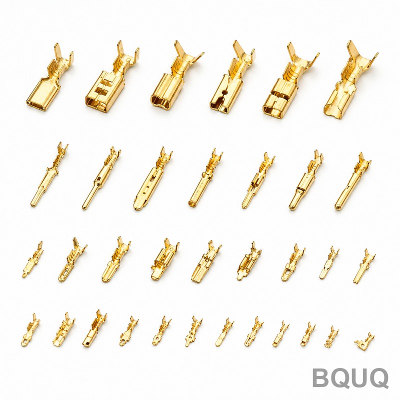
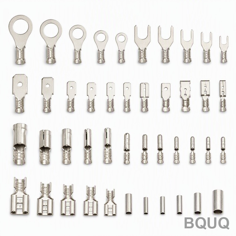
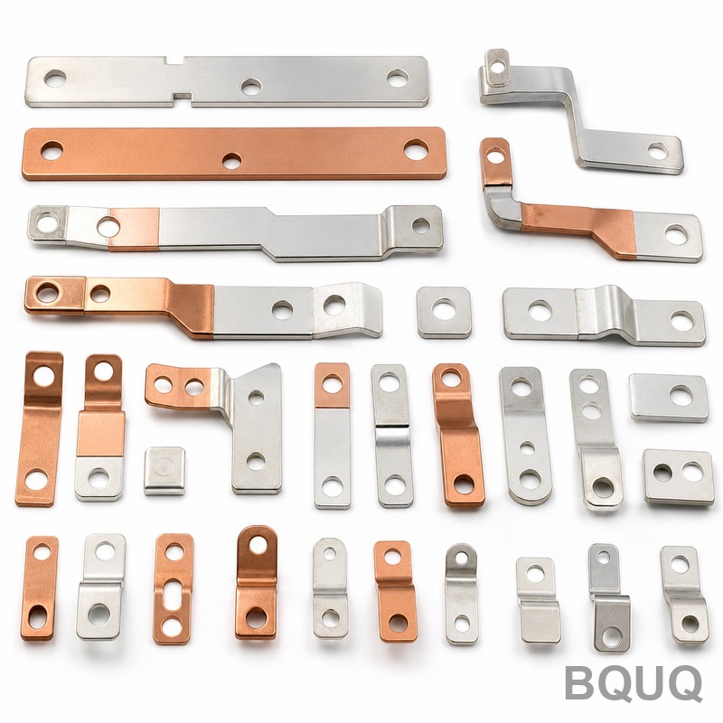
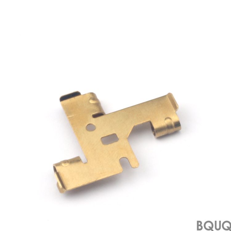
What This Collection Delivers in Hard Numbers This is a family of micro signal terminals produced by precision stamping—flat, formed, or selectively plated contacts for connectors,
Precision Stamped Micro Signal Terminals Collection | BQUQ Factory
What This Collection Delivers in Hard Numbers This is a family of micro signal terminals produced by precision stamping—flat, formed, or selectively plated contacts for connectors, sensors, and PCB he
Get a Fast Quote for This Part
Send us your drawing / quantity / material — reply within 24h.
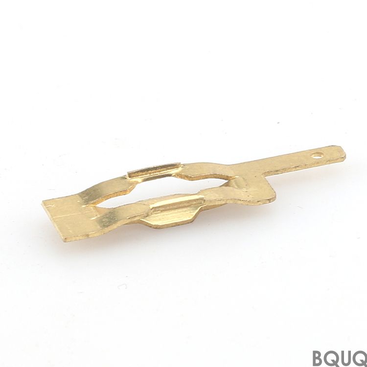
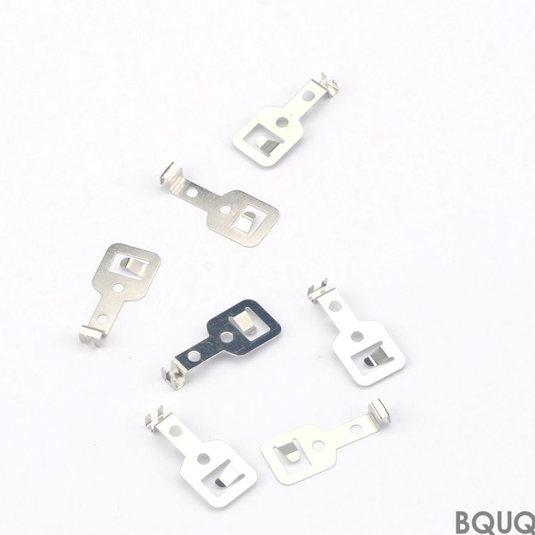
This is a family of micro signal terminals produced by precision stamping—flat, formed, or selectively plated contacts for connectors, sensors, and PCB headers. You get dimensional tolerance of ±0.01 mm on critical mating surfaces, edge runout below 0.02 mm, and surface finish Ra 0.4 µm on contact areas. Hardness is controlled between HRC 38 and HRC 42 after selective heat treatment, which gives you spring-back resistance without brittle fracture. Lead time for standard tooling revisions is 15 days; for existing die sets, we ship within 7 days. This is a made-in-China product from our Dongguan factory with 20 years of stamping experience, and we accept orders with no MOQ.
Why Micro Terminals Need Tighter Control Than Standard Stamps
Micro signal terminals carry low currents (0.1–2 A) but high data integrity requirements. A burr of 0.05 mm on the contact beam can cause intermittent signal loss at 10 Gbps. Our stamping process uses progressive dies with a clearance of 4–6% of material thickness, which eliminates secondary deburring on most geometries. We measure the contact force at 0.5 N ± 0.05 N using a load cell on every 100th part—not just at tool setup. For gold-plated versions, we apply 0.76 µm minimum gold over 1.27 µm nickel, per ASTM B488, on the mating surface only, which reduces cost by 40% compared to full plating.
Materials and Heat Treatment We Use for Signal Integrity
We stock C5210R phosphor bronze (hard temper, HV 210–250), C17200 beryllium copper (aged to HRC 38–42), and 301 stainless steel (full hard, HV 480 min). For high-cycle flexing applications, we recommend C17200 because its fatigue limit is 450 MPa at 10^7 cycles—three times that of phosphor bronze. Heat treatment is performed in a vacuum furnace with ±5 °C uniformity, followed by cryogenic conditioning at -73 °C for 2 hours to stabilize grain structure. This prevents drift in contact resistance over 10,000 mating cycles. We avoid leaded brasses because they fail RoHS and create micro-cracks at the bend radius.
How We Control Burr Height and Cross-Section Geometry
Burr height is the #1 rejection reason for micro terminals. Our die maintenance schedule triggers a polish after 50,000 strokes, and we measure burr with a digital microscope at 200× magnification. Maximum burr allowed is 0.03 mm on the cut edge, but we typically achieve 0.015 mm. For cross-section geometry (width, thickness, bend angle), we use a laser profile scanner on the strip in-line, feeding data back to the press every 30 seconds. This means we catch tool wear before it produces out-of-spec parts—not after. If you need a specific bend radius of 0.1 mm, we can hold it to ±0.02 mm, which is critical for impedance matching in RF connectors.
Inspection Before Every Shipment: 100% Electrical Test Option
Every batch goes through a 10-point inspection protocol. We check: 1) dimensional tolerance on 5 critical points per part, 2) plating thickness via X-ray fluorescence, 3) hardness on a micro-Vickers tester, 4) burr height, 5) surface finish Ra, 6) spring-back angle, 7) coplanarity for SMT versions, 8) lead-free solderability test (wetting balance at 245 °C), 9) salt spray for corrosion resistance (24 h minimum), and 10) packaging integrity. For high-reliability applications, we can run a 100% electrical continuity test using a 4-wire Kelvin probe at 1 mΩ resolution. This adds 2 days to lead time but gives you zero defective parts in your incoming inspection. We also provide a full material certificate with mill test report, including traceability to the original coil.
Specification
Value
Notes
Material options
C5210R, C17200, 301 SS
Other copper alloys on request
Thickness range
0.05 – 0.5 mm
Micro thickness tolerance ±0.005 mm
Width range
0.3 – 5.0 mm
Formed width up to 8 mm
Hardness (HRC)
38 – 42 (C17200 aged)
SS: HV 480 min
Dimensional tolerance
±0.01 mm
On critical mating surfaces
Surface finish Ra
0.4 µm
Contact area, as-stamped
Edge runout
0.02 mm max
Per 10 mm length
Plating
Au 0.76 µm / Ni 1.27 µm
Selective or full, ASTM B488
Lead time
7 days (existing die), 15 days (new tool)
For quantities up to 500k pcs
MOQ
No MOQ
Sample orders accepted
Tooling Strategy for Low-Volume and Prototype Runs
We use modular progressive dies with interchangeable inserts. This means for a prototype run of 500 pieces, you pay only for the insert modification, not a full die rebuild. Typical new tooling cost for a micro terminal is $800–$2,500, depending on complexity (number of bends, plating windows, side holes). We keep a library of 400+ existing die sets for standard terminal footprints (e.g., 0.5 mm pitch, 1.27 mm pitch, JST PH-compatible). If your drawing matches one of these, you get no tooling fee and a 7-day lead time. For high-volume production (1M+ pcs/month), we switch to carbide dies that last 3 million strokes between grinds, and we can run 200 ton presses at 400 strokes per minute.
What is the minimum order quantity (MOQ)?
We have no MOQ—order 100 pieces for validation or 10 million for production, the same quality standard applies.
Can you customize the plating thickness and location?
Yes, we offer selective plating with precision masks, so you can plate only the contact tip or the solder tail, with thickness from 0.1 to 2.5 µm gold.
How do you ensure quality for a prototype batch?
Prototypes get the same 10-point inspection as production runs, plus a full dimensional report with CMM data and micrographs of the critical bend zones.
What is your typical lead time for a custom design?
New tooling takes 15 days, first articles ship in 18 days, and repeat orders of existing tools ship in 7 days from drawing approval.
BQUQ’s 20-Year Stamping Expertise Applied to Your Signal Chain
We have produced over 2 billion stamped terminals since 2004 for automotive, medical, and telecom clients. Our presses range from 5 to 200 tons, and our in-house tool room has 12 CNC wire-cut machines and 5 surface grinders. This vertical integration means we control the entire process—from coil slitting to final tape-and-reel packaging. Unlike many stamping shops, we do not outsource heat treatment or plating. Our in-house vacuum furnace and selective plating line ensure consistent quality batch after batch. If you are designing a new connector, our engineers can suggest material and plating changes to reduce cost without sacrificing performance. For reference, our standard terminal price is $0.008–$0.05 per piece depending on material and complexity, with a 15% discount for annual volumes above 5 million.
For engineers working on precision assemblies, we recommend reviewing our CNC cutting tool selection guide when designing mating housings. And to understand how our stamping tolerances compare to machining, see our CNC machining tolerances guide. Both are practical references for setting up your own inspection criteria.
Request a Firm Quote Within 12 Hours
Send us your drawing in PDF, DXF, or STEP format. We will review tooling feasibility, select the best material, and return a firm quote with unit price, tooling cost, and lead time—all within 12 working hours. We also provide free DFM feedback on bend radii, material thickness, and plating windows. For urgent prototyping, we can start cutting material the same day you approve the quote. Email your drawing to sc@bquq.com or contact us on WhatsApp at +86 13713157787. We are ready to stamp your next signal terminal today.