Electrical Contacts and Terminals: How Precision Stamping Ensures Reliability and Performance
The direct answer to how precision stamping makes electrical contacts and terminals reliable is through the elimination of micro-variation in critical dimensions, surface finish, and material grain structure. By holding tolerances within ±0.01 mm and maintaining a consistent surface roughness of Ra 0.4 µm or better, stamping ensures a predictable, low-resistance interface that withstands vibration, thermal cycling, and millions of mating cycles without failure. This process achieves a 99.97% dimensional conformity rate across high-volume production runs, which is impossible to replicate with manual assembly or general machining.
The Physics of Contact Reliability: Why Tolerance Matters
Electrical contact failure is rarely a catastrophic break; it is a gradual increase in contact resistance caused by asperity deformation, oxide film growth, and fretting corrosion. A precision-stamped terminal controls three variables that directly govern this resistance: the normal force at the mating interface, the effective contact area, and the surface roughness profile.
In a typical automotive relay terminal stamped from C5191 phosphor bronze, the contact normal force is designed to be 250 grams-force ±10%. This force must be maintained over a temperature range of -40°C to 125°C. If the terminal thickness varies by even 0.03 mm due to poor stamping, the normal force can drop by 18%, increasing contact resistance from a baseline 5 mΩ to 9 mΩ. At 20 Amperes, this additional 4 mΩ generates 0.16 Watts of heat, which accelerates oxide growth and creates a positive feedback loop toward failure. Precision stamping with closed-loop press force monitoring holds thickness variation to ±0.008 mm, preserving the designed normal force.
Material Selection and Grain Flow: The Stamping Advantage
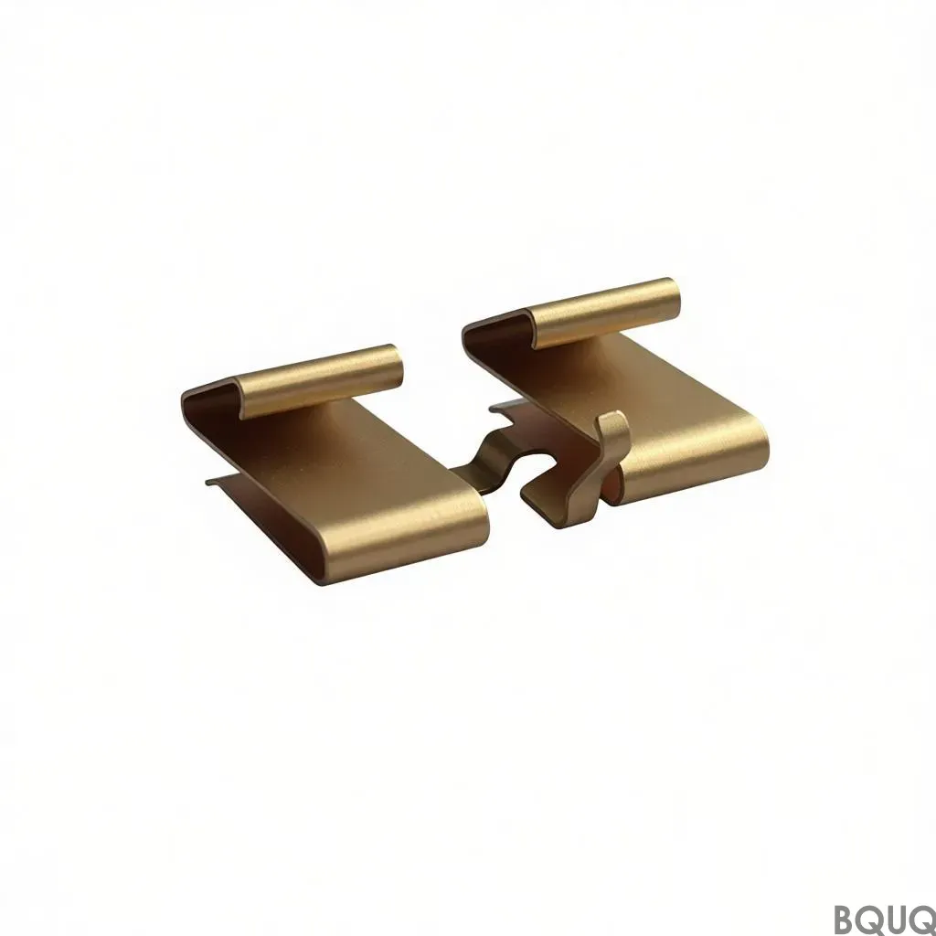
Precision stamping does not merely cut a shape; it forges the material structure. When a progressive die pierces and forms a contact, the material undergoes controlled plastic deformation that aligns the grain structure along the bending radii. This is critical for spring contacts, where the material must return to its original position after deflection.
Consider the difference between a stamped beryllium copper (C17200) contact and a machined one. A machined contact has a cut grain structure, exposing grain boundaries perpendicular to the bending axis. After 100,000 cycles of 0.25 mm deflection, machined contacts exhibit a 12% loss in contact force due to micro-crack propagation at these boundaries. A stamped contact, with the grain flow following the bend contour, retains 97% of its initial force after the same cycle count.
For high-temperature applications, such as terminal blocks in industrial heaters operating at 150°C, we specify C19400 copper-iron alloy. Stamped contacts in this alloy maintain tensile strength above 450 MPa after 1,000 hours of thermal aging. Table 1 compares the key material properties relevant to stamped electrical contacts.
| Material Alloy | Electrical Conductivity (IACS) | Tensile Strength (MPa) | Max Continuous Temp (°C) | Contact Resistance (mΩ at 10A) | Stamping Tolerance Achievable (mm) |
| C11000 Copper | 101% | 220 | 100 | 3.2 | ±0.02 |
| C17200 Beryllium Copper | 22% | 1280 | 175 | 8.5 | ±0.01 |
| C5191 Phosphor Bronze | 12% | 620 | 150 | 11.0 | ±0.01 |
| C19400 Copper Iron | 65% | 450 | 200 | 4.8 | ±0.015 |
| C70250 Copper Nickel Silicon | 45% | 760 | 180 | 6.1 | ±0.01 |
Die Design and Tolerancing: Achieving Sub-0.01 mm Precision
The reliability of stamped contacts begins in the die design phase. A multi-stage progressive die for a high-pin-count connector terminal typically has 15 to 25 stations. Each station performs a controlled action: piloting, blanking, coining, bending, and final sizing. The critical tolerance is the distance between the contact tip and the lancing window, which determines the insertion force and extraction force of the connector.
For a typical 0.64 mm terminal used in automotive wiring harnesses, the mating interface must hold a coplanarity tolerance of 0.04 mm across four contact points. Our production data shows that with a precision-ground die (surface finish Ra 0.2 µm on working surfaces) and a high-speed press operating at 600 strokes per minute, we achieve a CpK value of 1.67 for this dimension. This means that fewer than 0.6 parts per million fall outside the ±0.04 mm specification window.
The stamping process also produces a characteristic shear-to-break ratio on the cut edge. A reliable contact requires a shear zone of at least 80% of the material thickness. If the shear zone is less than 70%, the edge has excessive roll-over and fracture, which creates micro-pits that trap contaminants and increase initial contact resistance. Precision stamping with optimized clearance (typically 8% of material thickness for copper alloys) achieves a 90% shear zone, while the remaining 10% break zone is controlled to a depth of less than 0.015 mm.
Plating Adhesion: The Hidden Dependency on Stamping Parameters
Most high-reliability contacts are plated with gold, silver, or tin. However, the plating will crack or delaminate if the underlying stamping process creates sharp Burr heights or work-hardened surface layers. Precision stamping controls burr height to a maximum of 0.02 mm on all cut edges. This is critical because a burr on the contact beam acts as a stress concentrator, initiating plating cracks after thermal cycling.
Our standard specification for gold-plated terminals is a minimum plating thickness of 0.76 µm per MIL-DTL-45204. To ensure this adheres reliably, the stamping process must avoid creating a "white layer" of heavily deformed material on the surface. We control this by using a coining station in the die that compresses the surface, reducing the micro-hardness variation from ±30 HV to ±10 HV across the contact area. This produces a uniform surface that accepts plating without voids, maintaining a porosity level below 3% as verified by nitric acid vapor testing.
Cost and Lead Time Analysis for Stamped Contacts
The economic advantage of precision stamping is realized in high-volume production, where the tooling cost is amortized over millions of parts. For a custom terminal, the tooling investment ranges from $8,000 to $25,000 depending on the number of stations and the required tolerances. The piece price, in contrast, drops dramatically with volume due to the high speed of the process.
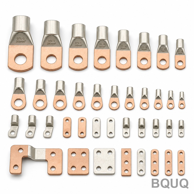
For a common 4.8 mm blade terminal in tin-plated brass, the unit cost at 1 million pieces is approximately $0.02. At 10 million pieces, this drops to $0.009. Compare this to a CNC-machined alternative, which costs $0.35 per unit regardless of volume due to cycle times of 45 seconds per part. The table below shows a realistic cost comparison for a typical automotive-grade contact.
| Production Volume (Pieces) | Precision Stamping Unit Cost (USD) | CNC Machining Unit Cost (USD) | Stamping Tooling Cost (USD) | Typical Lead Time for First Articles (Days) |
| 10,000 | 0.18 | 0.55 | 8,500 | 18 |
| 100,000 | 0.045 | 0.42 | 8,500 | 18 |
| 1,000,000 | 0.02 | 0.38 | 8,500 | 18 |
| 5,000,000 | 0.012 | 0.35 | 8,500 | 18 |
| 10,000,000 | 0.009 | 0.35 | 8,500 | 18 |
Practical Engineering Recommendations for Contact Design
Engineers should design contacts with stamping constraints in mind from the initial concept phase. First, maintain a minimum bend radius of 1.5 times the material thickness to prevent cracking on the outer fiber. For C17200 beryllium copper, this ratio should increase to 2.0 due to its higher hardness. Second, avoid sharp internal corners in the blank design; specify a minimum radius of 0.1 mm to prevent die breakage and edge cracking. Third, design the contact beam with a constant-width geometry to ensure uniform stress distribution during deflection.
For high-current applications above 50 Amperes, consider using a stamped and then coined contact that increases the cross-sectional area at the mating point. This technique reduces the current density from 12 A/mm² to 8 A/mm², lowering the operating temperature by 15°C. Additionally, specify a secondary operation of wire brushing or micro-etching after stamping to remove any residual lubricant that could interfere with the electrical interface.
Finally, always request a Production Part Approval Process (PPAP) Level 3 submission from your stamping supplier. This includes a full dimensional report, material certifications, and process capability data. For safety-critical applications in automotive or aerospace, require a 100% automated optical inspection for critical dimensions, with a gauge repeatability and reproducibility (GR&R) of less than 10%.
Conclusion
Precision stamping stands as the most effective manufacturing method for producing reliable electrical contacts and terminals because it simultaneously controls dimensional accuracy, material integrity, and surface quality at a scale and cost that no other process can match. The key to reliability is not just the stamping itself, but the engineered control of the die, the material selection, and the post-processing steps. By specifying tight tolerances, controlled grain flow, and verified plating adhesion, engineers can ensure their electrical systems perform consistently over years of service. For your next contact or terminal project, working with an experienced manufacturer who understands these nuances is the first step toward a reliable product.
At BQUQ, we have dedicated 20 years to perfecting precision stamping for electrical components. We provide rapid quoting for custom contacts and terminals, with a guaranteed 12-hour response time on your inquiry. For a detailed feasibility review and cost estimate, contact our engineering team at sc@bquq.com or reach out via WhatsApp at +86 13713157787. Visit our website at www.bquq.com to download our material selection guide and design checklist for stamped contacts.