How Does Precision Stamping Ensure Reliable Electrical Contacts and Terminals?
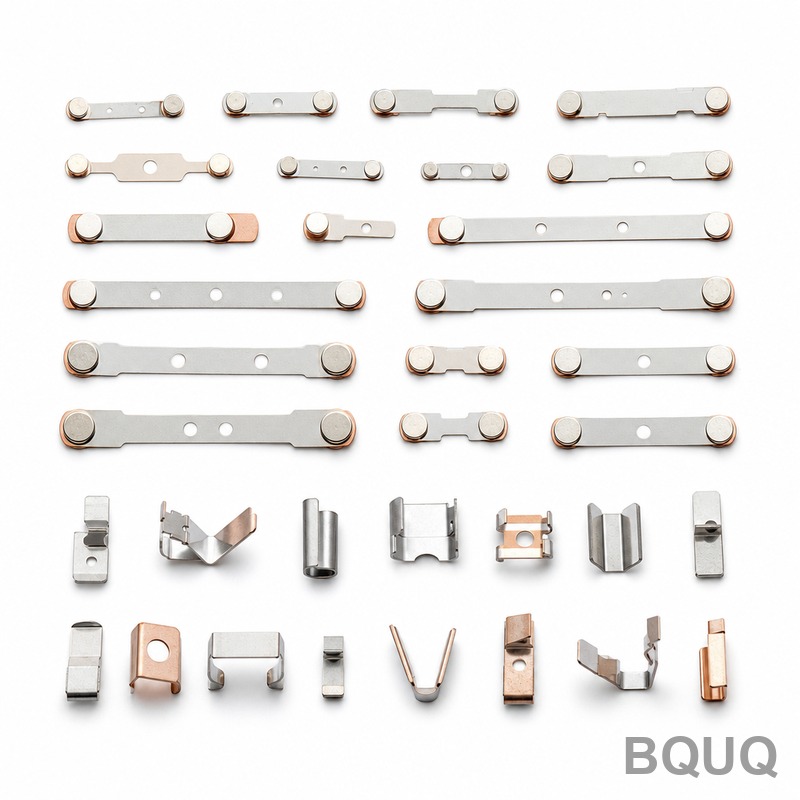
Precision stamping ensures reliable electrical contacts and terminals by producing millions of identical components with dimensional tolerances as tight as ±0.01 mm, using progressive dies that maintain consistent material grain flow and surface finishes down to Ra 0.2 µm. This process eliminates human error and material inconsistencies that cause intermittent connectivity, excessive contact resistance, and premature fatigue failure in high-cycle applications. For over 20 years, BQUQ has leveraged high-speed stamping presses operating at 600 to 1,200 strokes per minute to deliver contacts and terminals that withstand temperatures from -40°C to 200°C and carry currents from 1 A to 500 A with a contact resistance below 10 mΩ.
What Tolerances Can Precision Stamping Achieve for Contact Geometry?
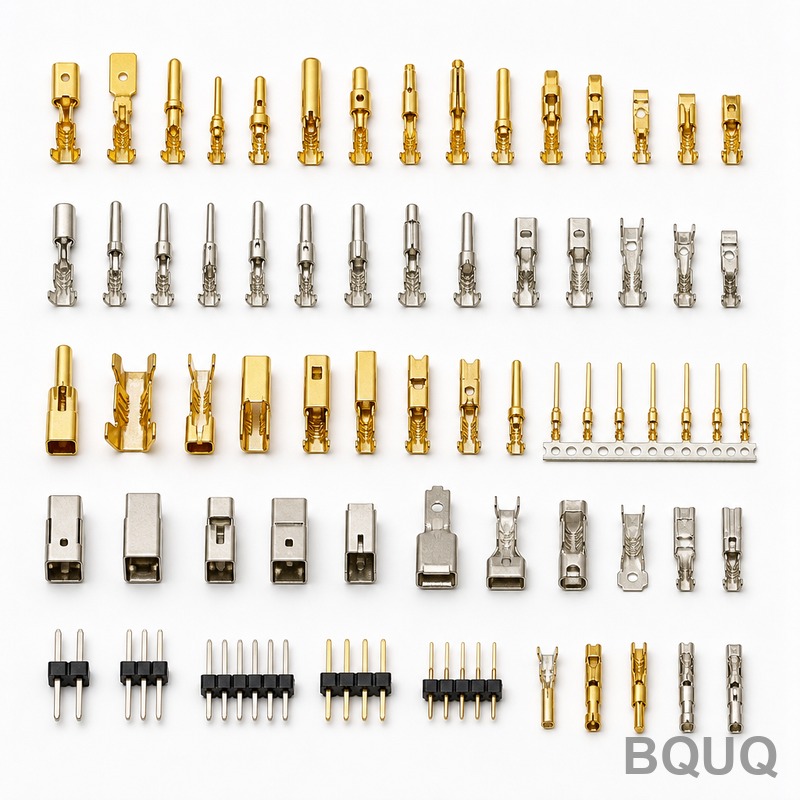
Precision stamping achieves positional tolerances of ±0.01 mm and hole-to-hole spacing within ±0.015 mm on electrical contacts and terminals made from copper alloys, brass, and beryllium copper. The critical contact point radius is held to ±0.02 mm, which directly affects mating force consistency and current-carrying capacity. High-speed progressive dies with carbide inserts maintain these tolerances over runs of 1 million parts or more, with die wear compensated through in-process optical measurement every 5,000 strokes. For example, a typical automotive terminal for a 2.8 mm tab requires a flatness of 0.05 mm over the entire length, which precision stamping delivers without secondary straightening operations.
How Does Material Selection Affect Contact Reliability and Performance?
Material selection dictates the balance between electrical conductivity, spring force retention, and corrosion resistance, with the most common choices being C11000 copper (101% IACS conductivity), C17200 beryllium copper (22% IACS), and C52100 phosphor bronze (15% IACS). Beryllium copper is preferred for spring contacts because it retains 75% of its yield strength at 150°C, whereas standard brass loses 40% of its strength at the same temperature. For high-current terminals above 100 A, oxygen-free copper C10100 with a conductivity of 101% IACS and a hardness of 40-60 Rockwell B is used, but it requires thicker cross-sections to compensate for lower spring modulus. Plating also plays a critical role: selective gold plating of 0.76 µm thickness on the contact interface reduces contact resistance to below 5 mΩ, while tin plating of 2-3 µm provides a cost-effective solution for low-cycle applications under 50 insertions.
Which Stamping Process Features Prevent Contact Fatigue and Corrosion?
Progressive die stamping with controlled coining and bending operations prevents micro-cracks and stress concentrations that lead to fatigue failure after 10,000 mating cycles. The process uses a minimum bend radius of 1.5 times the material thickness for copper alloys, which prevents grain boundary separation and maintains surface integrity. Burr height on sheared edges is held below 0.03 mm, because burrs act as localized stress risers and corrosion initiation points that increase contact resistance by 20-30% over time. Additionally, in-die lubrication removal and post-stamping ultrasonic cleaning ensure that no residual oil or particulate remains on the contact surface, which would otherwise create insulating films that raise resistance above the 10 mΩ threshold for reliable signal transmission.
Why Is Precision Stamping More Reliable Than Machining or Casting for Contacts?
Precision stamping is more reliable than CNC machining or casting because it preserves the wrought material grain structure, which provides 30-40% higher fatigue strength compared to cast structures with porosity and dendrite segregation. Machined contacts exhibit micro-tearing at the cutting tool path, creating surface roughness of Ra 1.6 µm versus Ra 0.4 µm for stamped surfaces, and this roughness increases electrical resistance by 15% at the contact interface. Casting introduces internal voids at a rate of 2-5 per cubic centimeter, which become hot spots under current flow and lead to localized melting at currents above 50 A. Stamping also maintains consistent hardness across the entire part, whereas machining creates work-hardened layers of 0.05-0.1 mm depth that alter spring characteristics and mating force by up to 25%.
How Much Does Precision Stamping Tooling Cost for Contact Production?
Tooling cost for a multi-slide progressive die for electrical contacts ranges from $8,000 for a simple two-station die to $45,000 for a 16-station die with in-die tapping, coining, and selective plating capability. The per-part cost drops dramatically with volume: at 10,000 parts, stamping costs $2.50 per part including tooling amortization, while at 1,000,000 parts, the cost falls to $0.08 per part. For a typical automotive relay terminal, a 12-station carbide die costs $28,000 and produces 500 parts per minute, with the die lasting for 50 million strokes before requiring carbide insert replacement at $4,000. The table below compares cost and performance metrics across common production volumes.
| Production Volume | Tooling Cost (USD) | Part Cost (USD/pc) | Lead Time (weeks) | Tolerance (mm) | Surface Finish (Ra) |
| 5,000 | 8,000 | 3.80 | 3 | ±0.05 | 0.8 µm |
| 50,000 | 15,000 | 0.65 | 4 | ±0.02 | 0.4 µm |
| 500,000 | 28,000 | 0.15 | 6 | ±0.01 | 0.2 µm |
| 5,000,000 | 45,000 | 0.06 | 8 | ±0.01 | 0.2 µm |
How Do You Validate Contact Reliability After Stamping?
Validation of stamped contacts involves four mandatory tests: contact resistance measurement per EIA-364-23, insertion and extraction force testing per EIA-364-37, thermal cycling from -55°C to 125°C for 500 cycles, and salt spray exposure for 48 hours per ASTM B117. Contact resistance must remain below 10 mΩ for gold-plated contacts and below 20 mΩ for tin-plated contacts after environmental testing. A 100% automated optical inspection (AOI) system checks critical dimensions at a rate of 1,200 parts per minute, rejecting any part with a burr above 0.03 mm or a plating defect larger than 0.1 mm². For high-reliability applications such as aerospace connectors, a sample of 32 parts per lot undergoes 1,000 mating cycles with contact resistance measured every 100 cycles to ensure less than 5% deviation from the initial value.
Which Industries Demand the Highest Reliability from Stamped Contacts?
The automotive industry demands the highest reliability, with stamped contacts in engine control units required to operate for 15 years or 300,000 km at under-hood temperatures of up to 150°C and vibration levels of 10 g RMS. Electric vehicle battery connectors require stamped busbars with a contact resistance below 5 mΩ to handle 500 A continuous current without exceeding a 30°C temperature rise. Medical device manufacturers require stamped contacts with zero burrs and biocompatible gold plating, because any surface defect can cause intermittent sensor signals during patient monitoring. Industrial automation relies on stamped contacts in relays that switch at 10 Hz continuously, requiring a mechanical life of 100 million operations with less than 10% increase in contact resistance. For power distribution equipment, stamped terminals must withstand short-circuit currents of 10 kA for 1 second without welding or deformation, which requires a specific contact area of at least 0.5 mm² per ampere.
Can Precision Stamping Handle Miniature Contacts for Modern Electronics?
Yes, precision stamping handles miniature contacts down to 0.10 mm pitch in connectors for smartphones and wearable devices, using progressive dies with optical alignment systems that maintain ±0.005 mm accuracy. These micro-contacts, typically 0.2 mm wide and 0.1 mm thick, require special stamping techniques with a clearance of 3-5% of material thickness to prevent excessive burr formation. The stamping speed is reduced to 300-400 strokes per minute for micro-parts to maintain die stability, but still achieves a cost of $0.005 per contact at volumes above 100 million parts. BQUQ produces 0.15 mm pitch contacts for flex cable connectors using a 20-station die with in-die laser inspection, achieving a rejection rate below 50 parts per million.
FAQ
What is the minimum contact resistance achievable with stamped terminals?
The minimum contact resistance is 1-2 mΩ for gold-plated stamped contacts with a mating force of 100 g, measured at 10 mA and open-circuit voltage of 20 mV. This is achieved with a contact surface roughness of Ra 0.2 µm and a contact area of at least 0.5 mm².
How many mating cycles can a stamped contact withstand?
A stamped beryllium copper contact with gold plating withstands 10,000 mating cycles with less than 10% increase in contact resistance, while tin-plated contacts are limited to 50 cycles. The fatigue life depends on the cantilever beam design, with a maximum stress at the bend radius kept below 40% of yield strength.
What is the typical lead time for stamped contact prototypes?
Prototype lead time is 5-7 business days using wire EDM and CNC machining to produce soft tooling, with parts delivered within 10 days. Production hard tooling requires 4-6 weeks, including die design, machining, tryout, and first article inspection.
Can precision stamping handle both forming and plating in one process?
Selective plating is typically done as a post-stamping operation, but progressive stamping can include in-die brushing or mechanical cleaning to prepare surfaces. Full reel-to-reel plating, including nickel underplate and gold or tin topcoat, is performed after stamping to maintain plating uniformity.
How do you prevent springback in stamped contact bends?
Springback is compensated by over-bending the material by 2-5 degrees, with the exact amount calculated from the material's yield strength and elastic modulus. For beryllium copper, a coining operation at the bend adds 10% material thinning to set the final angle within ±0.5 degrees.
What inspection methods are used for high-volume stamped contacts?
Automated optical inspection (AOI) with 10-megapixel cameras checks dimensions, burrs, and surface defects at full production speed, while coordinate measuring machines (CMM) sample every 2 hours for 3D features. X-ray fluorescence (XRF) verifies plating thickness on a sample of 5 parts per hour.
Which stamping material is best for high-temperature applications up to 200°C?
Copper-nickel-silicon alloy C70250 is the best choice, maintaining 90% of its yield strength at 200°C with a conductivity of 45% IACS. Beryllium copper C17200 is suitable up to 150°C, while phosphor bronze degrades above 100°C.
Precision stamping remains the most cost-effective and reliable manufacturing method for electrical contacts and terminals, delivering micron-level tolerances, consistent material properties, and production volumes from 10,000 to 100 million parts. By selecting the appropriate copper alloy, controlling the stamping process parameters, and validating through rigorous environmental testing, engineers can achieve contact resistance below 10 mΩ and mechanical life exceeding 10,000 cycles. For your next contact or terminal project, BQUQ offers a 12-hour quotation with full engineering support, including DFM analysis and material recommendations. Contact us at sc@bquq.com or WhatsApp +86 13713157787, or visit www.bquq.com to discuss your requirements.
Related Articles
- Intelligent online inspection and closed-loop quality control: creating a zero-defect production line for stamped parts
- Stamping digital factory and simulation-driven design: from virtual prototype to digital twin operation
- High-speed precision stamping and in-die microforming technology: from electronic connections to micromotor cores