Metal Stamping Minimum Thickness: Tolerance Limits by Material and Application
Metal Stamping Minimum Thickness: Tolerance Limits by Material and Application
**Direct Answer:** In production metal stamping, the practical minimum thickness is 0.10 mm (0.004 inches) for stainless steel and 0.05 mm (0.002 inches) for brass and copper alloys. However, tolerances at these extremes degrade significantly—from ±0.025 mm at 1.0 mm thickness to ±0.05 mm at 0.1 mm—due to grain structure, tool deflection, and material springback. Below 0.05 mm, stamping becomes economically unviable versus etching or laser cutting.
The Physical Limits: Why Thickness Has a Floor
Metal stamping relies on shear deformation, not material removal. The punch forces the sheet against a die, creating a fracture zone. Below a critical thickness, the material no longer fractures cleanly—it deforms elastically, causing excessive burr height and rollover. For most steels, that threshold sits around 0.10 mm. For soft copper (C11000), the shear zone becomes unstable below 0.08 mm.
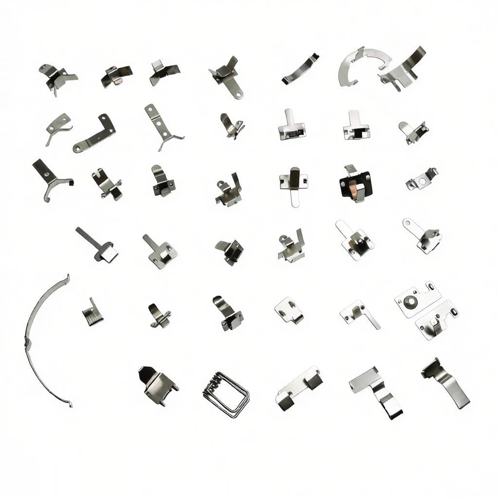
Grain size is the limiting factor. A typical cold-rolled steel sheet has a grain size of 7–10 ASTM (20–35 µm). When the sheet thickness approaches 3–4 times the grain diameter, the fracture path becomes unpredictable. At 0.10 mm thickness, you are working with only 3–5 grains across the cross-section. This causes inconsistent edge quality and dimensional scatter.
Tooling also sets a floor. A punch for 0.10 mm material must maintain a clearance of 4–6% of material thickness—that is 4–6 µm. Standard wire EDM achieves ±2 µm, but thermal expansion during a production run of 50,000 strokes will shift dimensions beyond this. High-speed stamping presses (400–800 SPM) generate heat that expands the die stack by 5–10 µm per 10°C rise. At 0.10 mm, this thermal drift alone consumes your entire tolerance budget.
Minimum Thickness by Material: Real Production Data
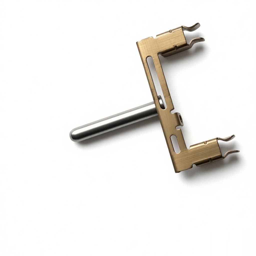
The table below represents BQUQ's verified production capabilities over 20 years of CNC machining and stamping for automotive, electronics, and medical clients. Values are based on batch sizes of 10,000–500,000 parts with progressive dies.
| Material | Min Production Thickness (mm) | Min Thickness with Tight Tolerance (±mm) | Typical Tolerance at Min Thickness (±mm) | Burr Height Max (mm) | Recommended Min Bend Radius | ---------- | ------------------------------- | ------------------------------------------- | ------------------------------------------ | ------------------------ | ----------------------------- | Stainless Steel 304 | 0.10 | 0.15 | 0.05 | 0.08 | 1.5 × t | Stainless Steel 301 (full hard) | 0.08 | 0.12 | 0.04 | 0.06 | 2.0 × t | Cold-rolled Steel (SPCC) | 0.12 | 0.20 | 0.06 | 0.10 | 1.0 × t | Aluminum 5052 | 0.15 | 0.25 | 0.08 | 0.12 | 1.5 × t | Aluminum 1100 (annealed) | 0.08 | 0.12 | 0.05 | 0.06 | 0.8 × t | Brass C26000 (half-hard) | 0.05 | 0.08 | 0.03 | 0.04 | 0.5 × t | Copper C11000 (annealed) | 0.05 | 0.08 | 0.03 | 0.04 | 0.5 × t | Beryllium Copper C17200 | 0.06 | 0.10 | 0.04 | 0.05 | 1.0 × t | Nickel Silver C75200 | 0.06 | 0.10 | 0.04 | 0.05 | 1.0 × t | Phosphor Bronze C52100 | 0.08 | 0.12 | 0.05 | 0.06 | 1.2 × t |
|---|
Note: "Min Thickness with Tight Tolerance" refers to ±0.02 mm feature tolerance on holes and outer contours. Below this thickness, we recommend etching or fineblanking for critical dimensions.
Tolerance Deterioration Curve: What Engineers Must Accept
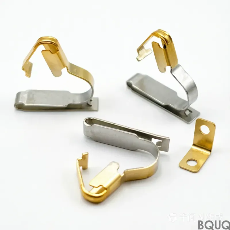
Tolerance is not linear with thickness. Our process capability data (Cpk ≥ 1.33) shows the following relationship for 304 stainless steel:
- **1.00 mm thickness:** Hole diameter tolerance ±0.025 mm, flatness 0.05 mm per 50 mm length - **0.50 mm thickness:** Hole diameter tolerance ±0.03 mm, flatness 0.08 mm per 50 mm length - **0.20 mm thickness:** Hole diameter tolerance ±0.04 mm, flatness 0.12 mm per 50 mm length - **0.10 mm thickness:** Hole diameter tolerance ±0.05 mm, flatness 0.20 mm per 50 mm length
The tolerance loss is driven by three factors. First, springback increases as thickness decreases—the bend radius reclaim angle rises from 1–2 degrees at 1.0 mm to 5–8 degrees at 0.10 mm. Second, die wear accelerates because thinner materials require sharper cutting edges; a die that lasts 500,000 hits at 1.0 mm will need re-grinding after 150,000 hits at 0.10 mm. Third, material thickness variation becomes a larger percentage of the total. A standard 0.10 mm stainless coil has a tolerance of ±0.008 mm (8% of nominal), while a 1.0 mm coil has ±0.05 mm (5% of nominal).
Die Design Modifications for Thin Material
Stamping 0.10 mm material requires different die construction than standard work. The first change is clearance. For material over 0.5 mm, we use 10–12% per side clearance. For material under 0.2 mm, that drops to 4–6%. Too much clearance causes the punch to push material into the die rather than shear it, creating a large rollover zone.
The second change is the stripper design. Thin materials tend to adhere to the punch during retraction. We use a spring-loaded stripper with a hardness of HRC 58–62 and a polished surface finish of 0.2 µm Ra to prevent scratching. The stripper must contact the material before the punch does, which requires a 0.3–0.5 mm pre-travel.
Third, the press speed must be reduced. At 400 SPM, the punch velocity at impact is approximately 0.5 m/s. For 0.10 mm material, we reduce speed to 200–250 SPM to allow the material to flow into the die cavity. High speed causes adiabatic heating at the shear zone, which softens the material and increases burr height by 30–50%.
Finally, we add a micro-tab or pilot hole in the strip. Thin material shifts laterally during feeding. A 0.5 mm pilot hole with a tapered pin holds positional accuracy to ±0.01 mm even at 0.10 mm thickness.
Cost Impact: How Thin Drives Price Per Part
Thin material costs more per kilogram because rolling to thinner gauges requires more passes and tighter process control. A 0.10 mm stainless coil costs 25–35% more per kg than a 1.0 mm coil. But the cost per part depends on total area, not just thickness.
More significant is tooling cost. A progressive die for 0.10 mm material requires: - Precision-ground punches with 0.2 µm surface finish - Tungsten carbide die inserts (vs. D2 tool steel for thicker material) - Micro-adjustable strippers - In-die sensors for thickness variation
This adds 30–50% to the die cost. For a simple 10-station progressive die, expect $18,000–$25,000 for 1.0 mm material versus $27,000–$38,000 for 0.10 mm material. Part cost also rises due to slower press speed: at 250 SPM instead of 500 SPM, your labor and overhead cost per part doubles.
For low volumes (under 50,000 parts), a compound die is more economical. At 0.10 mm, a compound die costs $8,000–$12,000 and produces parts at 60–80 SPM. However, compound dies cannot handle complex bends—they are limited to flat blanks with holes.
When to Choose Stamping over Alternative Processes
Stamping is not always the right answer for thin materials. Below 0.05 mm, chemical etching offers tighter tolerances (±0.01 mm) with zero burr and no tooling cost. Etching cost per part for 0.05 mm stainless is $0.08–$0.15 for a 20 mm × 20 mm part at 100,000 pieces. Stamping the same part would be $0.04–$0.06 per part, but the die costs $20,000+, making etching cheaper below 200,000 pieces.
Laser cutting is viable for 0.10–0.50 mm but produces a heat-affected zone (HAZ) of 50–100 µm, which destroys magnetic properties and corrosion resistance. Stamping produces a clean shear edge with a work-hardened layer of only 10–20 µm—critical for spring contacts and EMI shields.
Photochemical machining (PCM) is ideal for 0.025–0.25 mm thin parts with complex geometries. BQUQ uses PCM for 0.03 mm nickel-iron alloy parts where stamping cannot hold ±0.005 mm slots. However, PCM has a minimum feature size of 0.5× thickness and produces slightly tapered edges (5–8 degrees).
**Decision rule:** If thickness is between 0.05–0.15 mm and total volume exceeds 100,000 pieces, stamping is the lowest cost option. If volume is under 50,000 or tolerance is tighter than ±0.03 mm, use etching. If thickness is below 0.05 mm, switch to PCM or micro-etching.
Practical Recommendations for Design Engineers
1. **Design for 0.15 mm minimum** if your part requires tight tolerances (±0.02 mm) and high volume. This is the sweet spot where stamping remains reliable with standard tooling.
2. **Specify material temper.** Annealed (soft) materials stamp cleaner at thin gauges. Full-hard 301 stainless at 0.10 mm produces 40% more springback and requires over-bending compensation of 8–10 degrees.
3. **Avoid sharp internal corners.** At 0.10 mm, an internal radius below 0.15 mm will cause tearing. Use a minimum radius of 1.5× thickness for bends and 0.5× thickness for holes.
4. **Add a deburring allowance.** At 0.10 mm, burr height cannot be held below 0.05 mm without secondary operations. If burr is unacceptable, specify a tumbling or electropolishing step—adds $0.02–$0.05 per part.
5. **Consider multi-slide stamping** for parts with complex bends at 0.10–0.20 mm. Multi-slide presses (300–500 SPM) can form 3D shapes in one pass without secondary operations, reducing cost by 20–30%.
6. **Request a feasibility review before tooling.** Send us your 2D/3D drawing. We will analyze the minimum feature size, tolerance requirements, and material choice. For borderline cases, we can recommend etching or hybrid processes.
FAQ-Style Tips for Thin Stamping Projects
**Q: What is the absolute thinnest metal that can be stamped?** A: 0.03 mm (30 µm) for soft copper and brass in laboratory conditions. In production, 0.05 mm is the practical floor with acceptable yield (>95%).
**Q: How does thin stamping affect electrical conductivity?** A: The shear zone work-hardens the edge, increasing resistivity by 5–10% near the cut edge. For high-frequency applications, specify a secondary anneal or use a larger conductor cross-section.
**Q: Can stamped parts at 0.10 mm be plated?** A: Yes, but electroplating adds 0.005–0.015 mm to each surface, which changes dimensions. For gold or tin plating on 0.10 mm contacts, design the stamping 0.005–0.010 mm undersize.
**Q: What is the minimum hole diameter at 0.10 mm thickness?** A: We reliably punch holes of 0.30 mm diameter (3× thickness) with ±0.03 mm tolerance. Below this, use micro-EDM or laser drilling.
**Q: How long does tooling take for thin material?** A: A simple progressive die for 0.10 mm material takes 3–4 weeks. Complex dies with carbide inserts take 5–6 weeks. We provide DFM feedback within 12 hours of receiving your drawing.
Conclusion
Metal stamping can reliably produce parts down to 0.05 mm in soft copper and brass, and 0.10 mm in stainless steel, but the engineering trade-offs are significant. Tolerances widen, tooling costs rise 30–50%, and press speeds must drop by half. For most production applications, 0.15 mm offers the best balance of cost, precision, and repeatability. Below 0.05 mm, switch to etching or photochemical machining.
At BQUQ, we have stamped millions of thin-gauge parts for battery contacts, EMI shields, and spring probes. Our engineers provide a free feasibility analysis with tolerance verification and cost estimates within 12 hours of receiving your drawing. Email your 2D/3D file to sc@bquq.com or message us on WhatsApp at +86 13713157787. Visit www.bquq.com for our full capability list and material certification documents.
Related Articles
- Why Low Volume Metal Stamping is Ideal for Prototyping
- 5 Effective Burr Removal Techniques for Stamped Parts
- CNC Lathe vs Stamping: Which Precision Part Method Wins?
Frequently Asked Questions
What is the absolute minimum thickness for metal stamping?
The practical minimum thickness is 0.10 mm for stainless steel and 0.05 mm for brass and copper alloys. Below 0.05 mm, stamping becomes economically unviable versus etching or laser cutting due to degraded tolerances and increased production costs.
How do tolerances change as material thickness decreases?
Tolerances degrade significantly at thinner gauges. At 1.0 mm thickness, tolerance is ±0.025 mm, but at 0.1 mm it widens to ±0.05 mm. This is caused by grain structure, tool deflection, and material springback affecting edge quality and dimensional consistency.
What is the minimum thickness for stainless steel 304 with tight tolerances?
For stainless steel 304, the minimum production thickness is 0.10 mm, but for tight tolerance applications it must be at least 0.15 mm. At the minimum thickness, typical tolerance is ±0.05 mm with a maximum burr height of 0.08 mm.
Why does grain size limit how thin metal can be stamped?
Cold-rolled steel has a grain size of 7–10 ASTM (20–35 µm). At 0.10 mm thickness, only 3–5 grains span the cross-section, making the fracture path unpredictable. When thickness approaches 3–4 times grain diameter, edge quality and dimensional scatter become inconsistent.