Precision Stamping for Electrical Contacts: Reliability, Tolerances, and Cost Efficiency
Electrical contacts and terminals fail not because of material science limitations but because of manufacturing variance. Precision stamping delivers the repeatable dimensional control, surface finish, and metallurgical consistency required for reliable current transfer and mating cycle longevity. In high-vibration environments and high-temperature applications, a stamped contact with a tolerance of ±0.01 mm outperforms a machined part with ±0.05 mm because the stamped part maintains consistent contact force and lower electrical resistance across millions of cycles.
The Mechanical and Electrical Demands on Stamped Contacts
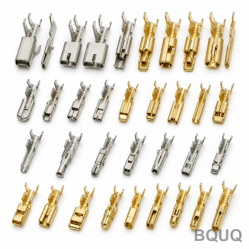
A contact terminal must satisfy three conflicting requirements: low electrical resistance, high mechanical strength, and resistance to environmental corrosion. Precision stamping addresses all three through controlled grain flow. When a strip of C11000 copper or C17200 beryllium copper is stamped, the material work-hardens along the bend radii, increasing tensile strength from 300 MPa to over 500 MPa in the formed zone. This localized strengthening is impossible to achieve with casting or machining.
The critical parameter is contact normal force, typically specified between 0.5 N and 5.0 N for signal contacts. This force is generated by the cantilever beam geometry of the stamped terminal. A variation of ±0.02 mm in beam thickness changes the normal force by approximately 15 percent. Precision stamping holds beam thickness to ±0.008 mm on strip stock, ensuring that contact resistance remains below 10 milliohms over the product lifetime. For power terminals carrying 20 A to 50 A, the stamping process maintains a consistent cross-sectional area that prevents localized hot spots.
Material Selection and Plating Strategies
The substrate material determines the base performance, while the plating determines the contact interface reliability. For automotive applications, C15100 copper-zirconium alloy provides a balance of conductivity (90% IACS) and softening resistance up to 380°C. For high-cycle connectors, C17200 beryllium copper offers 120,000 psi yield strength and maintains spring properties up to 200°C, but costs 3.2 times more than phosphor bronze.
Plating selection follows a performance hierarchy. Selective gold plating (0.76 μm minimum) over nickel is standard for signal contacts requiring under 20 milliohms and 500+ mating cycles. For power terminals, tin-lead or pure tin plating (2.5 μm to 5.0 μm) provides corrosion resistance but requires higher contact force to break through the oxide film. The stamping process must account for plating thickness variation; a tolerance of ±0.5 μm on selective plating prevents edge exposure and reduces material cost by 40 percent compared to full plating.
| Material Grade | Conductivity (% IACS) | Yield Strength (MPa) | Max Operating Temp (°C) | Relative Cost per kg |
| C11000 Copper | 101 | 70 | 150 | 1.0 |
| C15100 Cu-Zr | 90 | 290 | 380 | 1.4 |
| C26000 Brass | 28 | 120 | 130 | 0.8 |
| C51000 Phosphor Bronze | 15 | 340 | 175 | 1.6 |
| C17200 Beryllium Copper | 22 | 1100 | 200 | 3.2 |
Tolerance Control and Die Design for Consistent Contact Force
Reliability begins in the progressive die. For a typical stamped terminal with a 0.3 mm thick spring arm, the die must maintain a punch-to-die clearance of 4 percent of material thickness, which for 0.3 mm stock equates to 0.012 mm per side. This clearance directly affects the burnish-to-fracture ratio on the sheared edge. A 60 percent burnish zone ensures a flat, dense edge that resists fatigue cracking. BQUQ achieves this through CNC-ground die inserts with a surface finish of 0.2 μm Ra and laser-measured wear tracking after every 50,000 strokes.
The bending station is where most tolerance drift occurs. Springback for C17200 at a 90-degree bend is 2 to 4 degrees, requiring the die to over-bend by that amount. Since springback varies with strip hardness, BQUQ uses in-die sensors that measure the bend angle every 10th stroke and adjust the coining pressure automatically. This closed-loop control maintains the contact beam angle within ±0.3 degrees, which translates to a normal force variation of less than 7 percent. For reference, an uncontrolled stamping process typically exhibits 15 to 20 percent force variation.
Surface Finish and Contamination Control
Contact resistance is exponentially sensitive to surface contamination. A 1 μm particle of silicone oil on the contact surface increases resistance from 5 milliohms to 50 milliohms. Precision stamping mitigates this through three mechanisms. First, the die surface is coated with a diamond-like carbon (DLC) film that reduces friction and prevents material pickup, keeping the stamped surface roughness below 0.4 μm Ra. Second, the stamping process uses a low-residue lubricant that evaporates below 80°C, eliminating the need for aggressive chemical cleaning that could damage plating.
Third, the stamping environment is controlled. BQUQ operates its precision stamping presses inside a Class 100,000 cleanroom with temperature held at 23°C ± 1°C. This prevents condensation on the strip and minimizes airborne particle adhesion. The result is a contact surface that meets the requirements of EIA-364-23 for low-level contact resistance testing, with a maximum allowable resistance change of 5 milliohms after 100 hours of heat aging at 105°C.
Production Economics and Lead Time Comparison
Precision stamping becomes economically superior to other fabrication methods at volumes above 50,000 pieces. The tooling investment for a multi-station progressive die ranges from $8,000 to $25,000 depending on part complexity and number of stations. In contrast, CNC machining requires no tooling but has a unit cost that is 8 to 12 times higher. At 500,000 pieces, a stamped terminal costs $0.02 to $0.08 per piece, while the same machined part costs $0.25 to $0.60.
| Production Method | Tooling Cost (USD) | Unit Cost at 100k pcs | Lead Time for First Article | Tolerance Capability |
| Precision Stamping | 8,000 - 25,000 | 0.02 - 0.08 | 3 - 5 weeks | ±0.008 mm |
| CNC Machining | 0 - 2,000 | 0.25 - 0.60 | 1 - 2 weeks | ±0.015 mm |
| Metal Injection Molding | 15,000 - 40,000 | 0.05 - 0.15 | 6 - 8 weeks | ±0.030 mm |
| Photo Chemical Etching | 1,000 - 3,000 | 0.10 - 0.20 | 2 - 3 weeks | ±0.025 mm |
For a new product launch requiring 250,000 terminals, the total cost of ownership for stamping is $18,000 to $25,000 including tooling. Machining the same volume costs $62,500 minimum. The stamping tooling payback period is reached at approximately 60,000 pieces. For low-volume prototyping under 5,000 pieces, BQUQ recommends a hybrid approach: use CNC machined samples for functional testing, then transition to stamped production once the design is frozen.
Design for Stamping: Practical Guidelines
The most common cause of unreliable stamped contacts is a design that ignores the forming limits of the material. Minimum bend radius should be 1.0 times the material thickness for copper alloys and 2.0 times for beryllium copper to prevent cracking. The width-to-thickness ratio of the spring beam should be at least 3:1 to prevent twisting during bending. Grain direction matters: forming should occur perpendicular to the rolling direction to maximize ductility.
Hole placement is another critical factor. A hole edge must be at least 2.5 times the material thickness away from a bend line. Closer placement causes the material to thin and crack during forming. For terminals that require a locking lance or detent, the lance angle should be between 30 and 45 degrees, with a minimum material thickness of 0.25 mm for adequate stiffness. BQUQ provides a free design-for-manufacturing review and will suggest modifications that reduce tooling cost by up to 18 percent without compromising electrical performance.
Verification and Quality Control Methods
Reliability claims must be backed by data. BQUQ performs 100 percent dimensional inspection on critical features using a vision system with a measurement repeatability of ±0.002 mm. Every production lot undergoes a contact resistance test per EIA-364-23 using a four-wire Kelvin method at 10 mA and 20 mV open circuit. The acceptance criteria is 10 milliohms maximum for gold-plated contacts and 15 milliohms for tin-plated contacts. A sample from each lot is also subjected to a 500-cycle mating test to verify that the contact normal force degrades by no more than 20 percent from the initial value.
Environmental testing follows the automotive specification USCAR-21. This includes 1,000 hours of damp heat at 85°C and 85 percent relative humidity, followed by a 24-hour salt spray test. The stamped contacts must show no evidence of base metal corrosion on the contact interface after plating removal. For high-temperature applications, a thermal shock test from -40°C to +150°C for 500 cycles verifies that the material does not relax and lose contact force.
Conclusion and Engineering Recommendation
Precision stamping is the correct choice for electrical contacts and terminals when the annual volume exceeds 50,000 pieces, the tolerance requirement is tighter than ±0.02 mm, and the application demands consistent contact force over a wide temperature range. The process delivers a combination of dimensional accuracy, surface integrity, and cost efficiency that no other manufacturing method can match at scale. The key to reliability is not just the stamping press, but the entire system: die design, material selection, plating control, and environmental management.
For engineers evaluating a new or existing connector design, request a stamped prototype before finalizing the PCB layout. Stamped contacts have different coplanarity and standoff characteristics than machined components, which can affect solder joint reliability. BQUQ offers a free engineering consultation and a stamped sample within 12 hours of receiving your 2D drawing or 3D model. Send your requirements to sc@bquq.com or contact us on WhatsApp at +86 13713157787. Visit www.bquq.com to download our material and tolerance selection guide.
Related Articles
- Intelligent online inspection and closed-loop quality control: creating a zero-defect production line for stamped parts
- Stamping digital factory and simulation-driven design: from virtual prototype to digital twin operation
- High-speed precision stamping and in-die microforming technology: from electronic connections to micromotor cores