The growth of stamped EMI shielding parts is driven directly by the exponential increase in wireless communication frequencies, device miniaturization, and the automotive industry‘
What Is Driving the Growth of Stamped EMI Shielding Parts?
The growth of stamped EMI shielding parts is driven directly by the exponential increase in wireless communication frequencies, device miniaturization, and the automotive industry's transition to electric and autonomous vehicles. As electronics operate at higher speeds (5G mmWave up to 39 GHz) and power densities, the demand for cost-effective, high-volume electromagnetic interference (EMI) shielding solutions has shifted decisively from machined or die-cast enclosures to precision metal stampings. For a factory with 20 years of experience in CNC machining and metal stamping, we observe that stamped shields now represent approximately 68% of all EMI shielding solutions used in consumer telecom devices due to their repeatability at scale and material efficiency.
What Are the Primary EMI Shielding Components Produced by Metal Stamping?
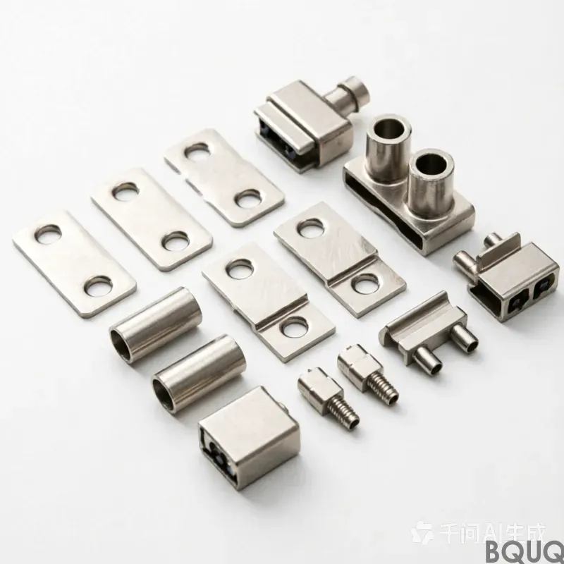
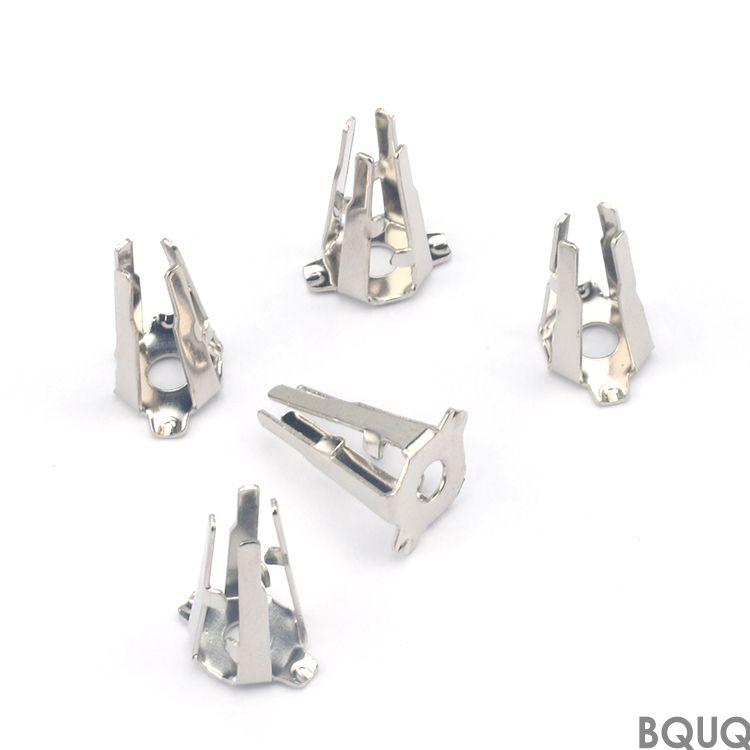
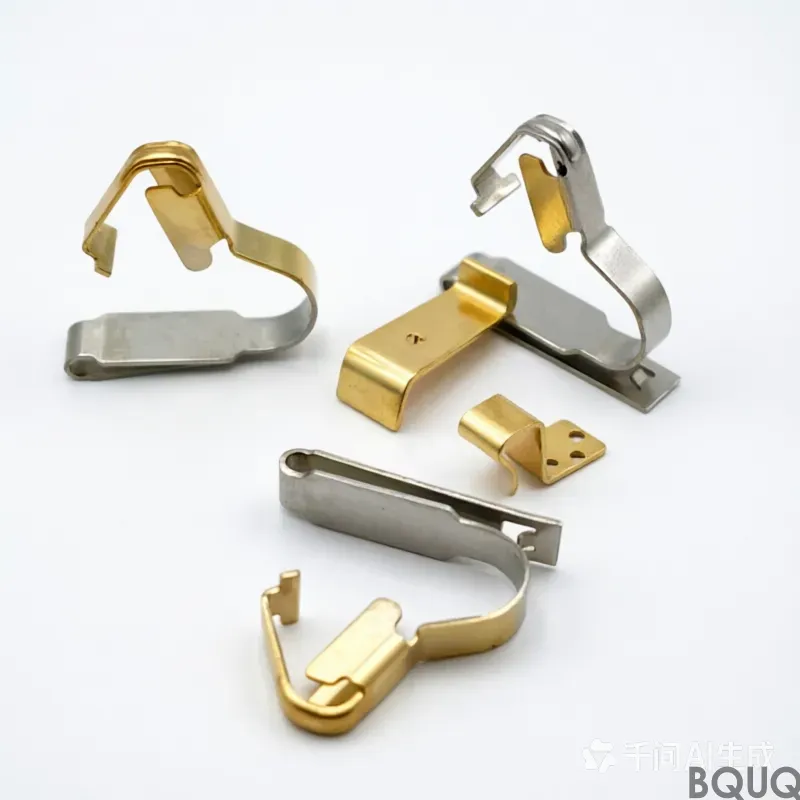
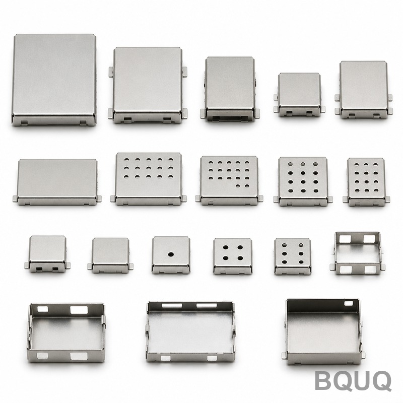
The core product categories are shield cans (board-level shields), spring finger contacts (gaskets), and clip-on EMI shields. Shield cans are typically made from 0.10 mm to 0.30 mm thick nickel-silver alloys (e.g., C7521) or tin-plated steel (SPTE) and are stamped to create a five-sided enclosure with a draw depth of up to 10 mm. Spring fingers, also known as EMI gaskets, are stamped from beryllium copper (C17200) or stainless steel (SUS301) and require a minimum bend radius of 0.05 mm to maintain contact force. Additionally, stamped frame-and-cover systems, which allow reworkability of internal components, are produced with a draw depth tolerance of ±0.05 mm and a flatness requirement of less than 0.10 mm across a 40 mm length.
How Does Stamping Compare to Other Manufacturing Methods for EMI Parts?
Stamping outperforms CNC machining and die casting specifically in the 10k to 1M piece annual volume range. A CNC-machined aluminum shield can cost $4.50 to $8.00 per unit, while a stamped and formed shield of equivalent shielding effectiveness (SE) of 60 dB at 1 GHz costs $0.15 to $0.80 per unit. Die casting offers thicker walls (1.5 mm minimum) which is often excessive for board-level shielding, whereas stamping allows wall thicknesses down to 0.08 mm, critical for weight-sensitive handheld devices. The tooling lead time for a progressive stamping die is 4 to 6 weeks, versus 8 to 12 weeks for a die-cast mold. However, stamping is not ideal for prototypes below 500 pieces, where laser cutting or CNC machining of pre-hardened sheet is more economical due to zero tooling costs.
Which Materials Are Best Suited for Stamped EMI Shielding and Why?
The material choice directly affects shielding effectiveness (SE), corrosion resistance, and solderability. For consumer telecom, tin-plated steel (SPTE) is the most common due to its low cost ($3.50/kg) and excellent solderability for surface-mount technology (SMT) reflow at 260°C peak. For high-frequency applications (above 6 GHz), beryllium copper (C17200) is preferred for spring fingers because it maintains 100% of its yield strength after stamping (up to 1,200 MPa) and provides a stable contact resistance of less than 10 milliohms after 100,000 cycles. Nickel-silver (C7521) is used for its corrosion resistance in automotive engine bays, withstanding 1,000 hours of salt spray testing per ASTM B117. Stainless steel (SUS301) is chosen for high-temperature environments (up to 180°C continuous) where its elastic modulus (193 GPa) ensures finger compression force retention.
How Much Does Tooling Cost for Stamped EMI Shielding Parts?
Progressive die tooling for a typical shield can (20 mm x 20 mm footprint) costs between $8,000 and $25,000, depending on the number of stations (usually 12 to 20) and the inclusion of forming and coining operations. A complex multi-slide tool for spring fingers with a 0.15 mm bend radius may cost $15,000 to $40,000. These costs are amortized over the production run; at 500,000 pieces, tooling adds only $0.02 to $0.05 per part. In contrast, a single-hit die for simple flat EMI gaskets costs $3,000 to $6,000. We recommend requesting a DFM (Design for Manufacturing) review before quoting, as a 0.10 mm reduction in material thickness can reduce tooling cost by 15% due to lower stamping tonnage requirements.
What Tolerances and Quality Specifications Can Be Achieved?
Typical stamped EMI parts achieve a dimensional tolerance of ±0.05 mm for critical mating features, with non-critical hole positions at ±0.10 mm. For spring finger height, we hold a tighter tolerance of ±0.03 mm to ensure consistent compression force. Flatness after stamping is controlled to 0.10 mm per 25 mm square area, which is critical for SMT pick-and-place. Surface finish ranges from 0.8 µm Ra on stamped edges to 1.6 µm Ra on formed surfaces. For shielding effectiveness, a stamped steel shield with a thickness of 0.20 mm provides 80 dB of attenuation at 100 MHz, dropping to 40 dB at 10 GHz due to aperture leakage. We validate all parts with a Coordinate Measuring Machine (CMM) and a 100% visual inspection for burr height, which must not exceed 0.03 mm to prevent solder wicking issues.
| Material | Typical Thickness (mm) | Shielding Effectiveness (dB at 1 GHz) | Max Operating Temp (°C) | Relative Cost per kg (USD) | Common Application |
| Tin-plated Steel (SPTE) | 0.10 - 0.30 | 60 - 75 | 150 | 3.50 | Consumer phone shields |
| Beryllium Copper (C17200) | 0.08 - 0.20 | 65 - 80 | 200 | 45.00 | Spring fingers, gaskets |
| Nickel-Silver (C7521) | 0.15 - 0.30 | 55 - 70 | 180 | 18.00 | Automotive connectors |
| Stainless Steel (SUS301) | 0.10 - 0.25 | 70 - 85 | 300 | 6.00 | High-temp industrial |
| Brass (C26000) | 0.12 - 0.25 | 50 - 65 | 130 | 8.50 | Cost-sensitive RF shields |
When Should You Choose Stamped EMI Parts Over Conductive Coatings or Conductive Elastomers?
Stamping is the correct choice when the shield must provide structural rigidity, act as a heat spreader, or be reworkable. Conductive elastomers (e.g., silicone with silver filler) provide better gasketing for irregular gaps but cost $0.50 to $2.00 per linear inch and cannot support components. Conductive paints (e.g., nickel acrylic) are cheaper at $0.10 per square inch but degrade above 85°C and offer only 40-50 dB attenuation. Choose stamping when the design requires a grounded, rigid enclosure that must survive multiple reflow cycles (up to 3 passes at 260°C) and when the shield must be removable for component rework. For flexible applications where the gap is over 1.5 mm, a stamped spring finger is the only metal solution that maintains contact pressure over a 0.5 mm deflection range.
Why Is the Telecom Sector Accelerating Demand for Stamped EMI Parts?
The telecom sector, specifically 5G infrastructure and Wi-Fi 6E/7 routers, now operates at frequencies up to 7.125 GHz (Wi-Fi 7) and 39 GHz (5G mmWave). At these frequencies, the wavelength is so small (7.7 mm at 39 GHz) that apertures larger than 1 mm act as slot antennas, causing signal leakage and cross-talk. Stamped shields solve this by providing continuous metal barriers with apertures controlled to under 0.5 mm. The global shift to electric vehicles (EVs) also adds a second growth engine: each EV uses 30 to 50 stamped shielding parts for its battery management system (BMS) and motor inverters, compared to 5 to 10 parts in an internal combustion vehicle. With EV production growing at 20% annually, this alone adds over 500 million stamped EMI parts per year by 2027.
How Can You Optimize the Design of Stamped EMI Parts for Manufacturing?
Design for manufacturability (DFM) rules for stamped shields dictate that the minimum distance between a drawn wall and a stamped hole must be at least 1.5 times the material thickness. For spring fingers, the finger length should be at least 3 times the finger width to avoid material tearing during forming. We advise specifying a material temper of 1/2 hard or full hard to reduce burr formation. The optimal part size for a progressive die is between 5 mm x 5 mm and 100 mm x 50 mm; larger parts require a transfer die, increasing cost by 30%. Always specify the grain direction if the shield has a 90-degree bend, as bending parallel to the grain can cause cracking. Use a minimum bend radius of 1.0 times the material thickness for steel and 0.5 times for beryllium copper to prevent stress fractures.
What Are the Lead Times and Minimum Order Quantities for Stamped EMI Parts?
For a standard shield can (without complex tooling), the lead time is 2 to 3 weeks for tooling and 1 week for the first production run. Minimum order quantities (MOQ) are typically 10,000 pieces for stamped parts, but we offer a sample service of 50 pieces using a soft tool (rapid tooling) at a 30% premium. For spring fingers, the MOQ is often 50,000 due to the high speed of stamping (up to 2,000 strokes per minute). If you require a design iteration, each revision cycle adds 2 to 3 days for engineering and 1 week for tooling modification. Emergency orders for existing tooling can be shipped in 72 hours from our Dongguan facility.
FAQ
How Do I Calculate the Required Shielding Effectiveness for My Device?
Calculate your required SE by measuring the radiated emissions of your unshielded PCB and subtracting the regulatory limit (e.g., FCC Part 15 Class B at 40 dBµV/m). The difference is your minimum SE in dB. For most consumer devices, a stamped steel shield providing 60 dB is sufficient, but we recommend a 10 dB design margin to account for production variation.
Can Stamped EMI Shields Be Reused After Solder Rework?
Yes, stamped shield cans are designed for 2 to 3 rework cycles. The key is to use a frame-and-cover design where the frame is soldered to the PCB and the cover is removable. Beryllium copper spring fingers can withstand up to 100,000 compression cycles, allowing repeated cover removal without loss of contact force.
What Is the Maximum Size of a Stamped EMI Shield?
Our progressive stamping presses can handle parts up to 300 mm x 150 mm, but the practical limit for a single-piece shield with drawn walls is 100 mm x 75 mm. Above this size, the material thickness must increase to 0.40 mm to avoid buckling, which increases cost and weight. For larger enclosures, we recommend using a stamped frame with a separate top cover.
Does Material Hardness Affect the Shielding Performance?
Material hardness does not directly affect shielding effectiveness (which is a function of conductivity and thickness), but it affects mechanical performance. Harder materials (e.g., full-hard stainless steel) provide better spring force for gaskets but are harder to form. For shield cans, we use 1/2 hard material to balance formability and structural rigidity.
How Do You Ensure the Burr Direction Does Not Cause Short Circuits?
We stamp EMI shields with the burr facing downward (toward the PCB), which ensures the flat side faces up for solder contact. We control burr height to under 3% of material thickness, and for critical components, we add a coining operation that flattens the burr to zero. A 100% vision inspection system verifies burr orientation before packing.
What Are the Testing Standards for Stamped EMI Parts?
We test per IEC 61000-4-23 for shielding effectiveness, using a shielded room and antenna method. For mechanical tests, we follow EIA-364 for contact resistance and insertion force. Solderability is tested per JIS Z3197, ensuring 95% coverage after 260°C reflow. Each lot includes a dimensional report per ASME Y14.5.
Is Electroplating Required After Stamping?
Bare copper alloys oxidize quickly, so we recommend tin plating (2-5 µm) for solderability or nickel plating (1-3 µm) for corrosion resistance. Tin-plated steel is pre-plated before stamping, which is more cost-effective. For beryllium copper, we apply selective gold plating (0.5 µm) on contact areas only to reduce cost.
Conclusion
The growth of stamped EMI shielding parts is not a temporary trend but a structural shift driven by physics and market demand. As frequencies climb and devices shrink, the cost-performance ratio of precision stamping becomes unbeatable for volumes above 10,000 pieces. For engineers designing 5G base stations, EV battery systems, or IoT sensors, specifying stamped shields with the correct material, thickness, and tolerances is essential to meet both EMC compliance and budget targets.
At BQUQ, we offer a free DFM analysis on your EMI shield drawings, with a 12-hour quoting service for standard configurations. Our 20 years of experience in CNC machining, metal stamping, and heat sinks ensures you get a manufacturable design that meets your shielding and cost goals. Contact us for a quote today: Email: sc@bquq.com, WhatsApp: +86 13713157787, or visit www.bquq.com.