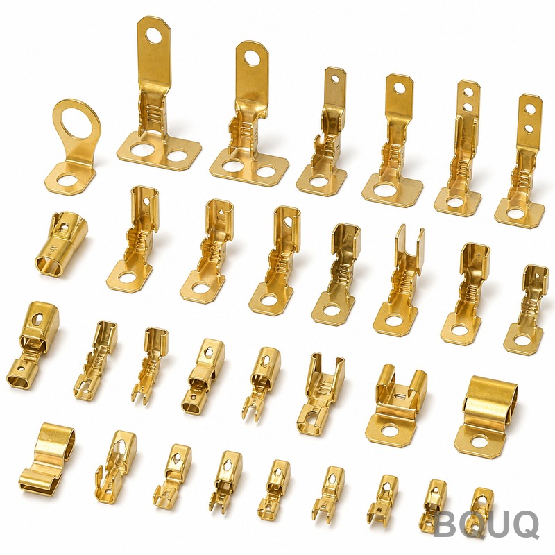
Data Center Busbar Stamping: T2 Copper 2mm, High-Conductivity, 100K/Month
A data center busbar carries the full fault current of a rack, and its stamped interface is where that current either passes cleanly or turns into heat. Two things decide the outcome: the conductivity of the copper and the quality of the stamped contact surface. Get either wrong and you get hot spots, rising voltage drop, and a part that fails thermal testing at exactly the wrong moment.
Project Background & Challenge
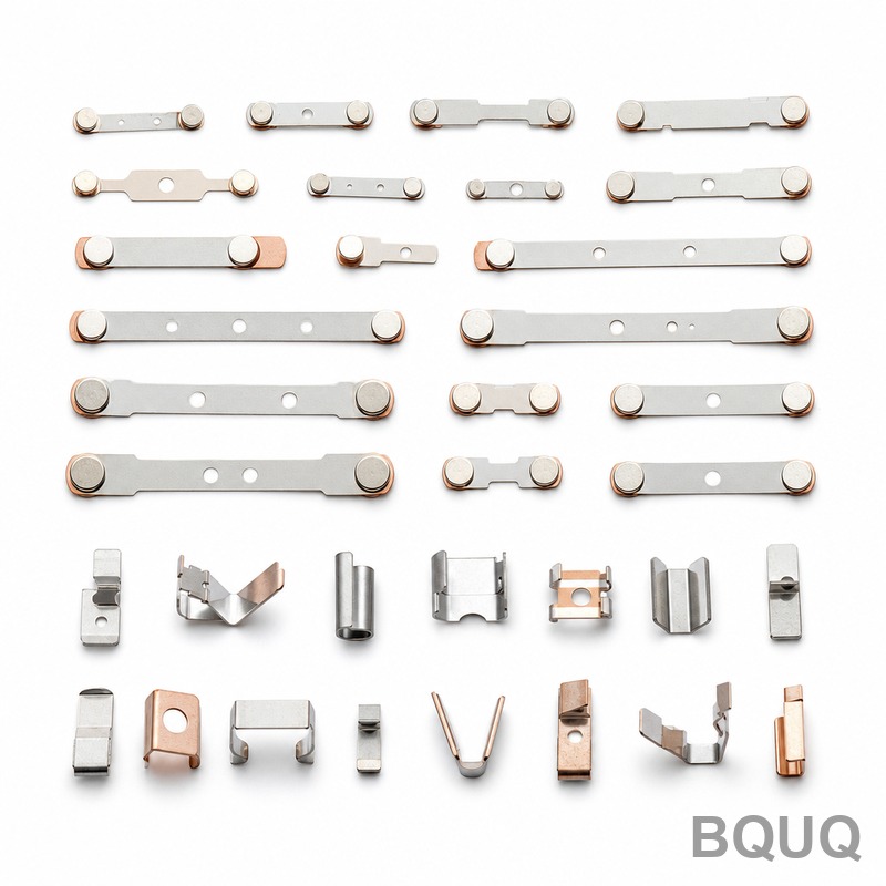
A data center power hardware vendor came to us with a family of stamped copper busbars for high-current power distribution inside racks and busway systems. The parts are formed from 2mm T2 copper strip, and at this thickness the material is stiff enough to fight the die, yet soft enough to deform where you do not want it. Volumes started at 100,000 pieces a month with a clear path to several times that as the platform rolls out.
The busbars must deliver low contact resistance at bolted and plug-in interfaces, hold flatness so they seat properly against mating components, and carry a tin plating that keeps the surface stable over years in a warm, continuously loaded environment. Any burr on a contact face, any crack at a bend, any variation in plating thickness becomes a reliability risk in a system nobody can afford to take offline for a single stamped part.
The technical challenge is that these requirements pull against one another during stamping. Higher-conductivity copper is softer and more prone to edge cracking and galling; tighter bend radii raise the risk of fracture on the outside of the bend; and a 2mm section means the die has to carry heavy tonnage while still producing a clean, burr-free shear on every contact edge. Add tin plating afterward and the cutting edges and flatness must already be right, because plating only amplifies whatever the stamping left behind.
Commercial pressure added a second constraint. The busbar family changes with every rack generation, so tooling had to be designed once and then produce consistently across long runs, while still allowing features to be revised between programs without scrapping the whole die. That meant predictable tool life, controlled burr, and a process that could be measured, not just run.
Material selection was fixed early: T2 copper, a high-conductivity grade that is the default for DC power hardware, at 2mm thickness to carry the current without excessive temperature rise. That choice, combined with the volumes, ruled out machining or casting and pointed squarely at progressive-die stamping as the only route able to hit cost and consistency at the same time.
BQUQ Process Solution
Overall: design a progressive die around the copper's real behaviour, control the forming in stages, and treat the contact surfaces as precision features rather than by-products of the stamping.
Progressive Die Design
The busbars run on a continuous progressive die so every feature, from pilot holes to contact profiles, bend lines, and the final trim, is set by the same tool in one pass, which keeps hole-to-edge relationships consistent across millions of strokes. The die is designed with staged forming so each bend takes a share of the deformation instead of one aggressive hit, which is what keeps 2mm T2 copper from cracking on the outside radius.
Forming, Bending & Deburring
Bend radii are set to match the material's real elongation rather than the drawing's minimum, and the shearing edges are maintained to produce a clean cut with minimal burr. After forming, parts pass through a controlled deburring step that removes sharp edges on the contact faces and bolt holes without rounding the features that need to stay crisp. Because the tool is progressive, the part is fully formed and separated in one continuous flow, which keeps cycle time low and dimensional consistency high at 100K pieces per month.
Tin Plating & Contact Resistance Control
Plating is where the busbar's long-term reliability is set. Parts are plated to a controlled thickness with good adhesion, and the process is monitored so the tin does not build unevenly on edges or hole walls, which is where contact resistance quietly climbs. Flatness is verified after plating, since a plated busbar that does not seat flat will read high resistance no matter how good the copper beneath it is. Nickel plating is available where a harder, more wear-resistant surface is needed for repeated mating cycles.
Key Specifications
| Item | Specification |
|---|---|
| Material | T2 copper strip, 2mm stock (0.1-3mm range available) |
| Forming | Progressive / continuous die stamping with staged bending |
| Hole positions | ±0.05mm, bend angle deviation within 0.5 degrees |
| Surface treatment | Tin plating (nickel plating available); plated flatness controlled |
| Contact resistance | Low and stable across batches, verified on the finished part |
| Volume | 100,000 pcs/month, scalable to multi-million volumes |
| Inspection | Per-lot dimensional check, plating thickness, and flatness verification |
| Delivery | Samples in 5 days, first production batch in 18 days |
Quality Control & Delivery
Before full production, a first-article inspection confirms the contact profiles, hole positions, bend angles, burr state, and plating thickness against the drawing. That signed-off first article becomes the baseline for the whole program, and it is re-checked whenever the die is serviced or a new coil lot is introduced.
In production, each lot carries a dimensional check with sampling, plating thickness verification, and a flatness check on the seating faces. Burr height and edge condition are watched because they drive contact quality. The full flow runs under an ISO9001:2015 quality system.
Result: samples in 5 days, first production batch in 18 days, and a stable process at 100,000 pieces a month that scaled to multi-million volumes as the customer's platform grew. Contact resistance stayed consistent lot to lot, and flatness held within the seating requirement after plating, which is what kept the parts off the customer's thermal-failure list.
Related Products & Resources
Stamped copper and brass parts for electrical duty are a regular request here. Related collections include Stamped Brass Electrical Terminals & Contacts and Stamped Hydrogen Fuel Cell Bipolar Plates, both sharing the same conductivity, flatness, and plating challenges as a busbar.
For process questions on stamping tolerances, plating, and volumes, see our FAQ Center, or send a drawing and we will return a quotation within 12 hours.
FAQ
Can you stamp 2mm T2 copper without cracking at the bends?
Yes, if the die is built for it. We stage the forming so each bend shares the deformation, set radii to match the copper's real elongation, and keep the shear edges sharp. The first article confirms the bend radius, burr, and plating before the run starts, and the process is watched lot to lot at 100,000 pieces a month.
How do you keep contact resistance low and stable?
By controlling the surface, not just the copper. Burr-free contact faces, uniform tin plating with good adhesion, and flatness verified after plating all keep the interface clean and consistent. Each lot is checked for plating thickness and flatness, which is where contact resistance problems usually start.
What volumes can a progressive die handle here?
Continuous-die stamping runs from 100,000 pieces a month upward to multi-million volumes, with stock thickness from 0.1mm to 3mm. The tooling is designed once and then produces consistently across long runs, so a ramping rack platform can scale without a new process every generation.
Do you offer tin and nickel plating on stamped copper?
Yes. Tin plating is standard for stable, solderable contact surfaces, and nickel plating is available where a harder, more wear-resistant face is needed for repeated mating. Both are thickness-controlled, and flatness is verified after plating so the part still seats properly against its mating busbar.