Solar Junction Box Terminal Stamping: T2 Copper 0.8mm Progressive Die, Tin-Plated, 1.5M pcs/month
A photovoltaic junction box terminal is one of those parts that looks trivial and quietly decides whether the whole module passes certification. It must carry high current for 25 years, strip insulation and pierce the bus wire in one crimp, and do all of this with contact resistance that never drifts from batch to batch. The hard part is not cutting copper - it is holding electrical consistency across a million pieces a month.
Project Background & Challenge
The customer is a solar module manufacturer in India, running multiple GW of annual cell-to-module capacity and supplying both domestic and export markets. Every junction box they build contains several stamped current-carrying terminals: the conductor strips that terminate the ribbon leads, form the spring contacts, and clamp onto the cable through an insulation-piercing crimp. A junction box carries and protects the module's entire electrical output, and under IEC certification rules the terminals inside it are treated as safety-critical components, so any sourcing change triggers a full re-qualification on the customer's side. The previous supplier produced acceptable first articles, but as volumes ramped toward a million pieces per month, three problems kept surfacing.
First, contact resistance varied. Terminal-to-terminal variation inside one junction box forced the customer to screen and re-test, and a small percentage of boxes still failed IEC continuity checks at final inspection - failures that arrived as a customer complaint from a project developer, not as an internal rejection, which made the cost far higher than the scrap value. Second, the tin coating was inconsistent - thinner on formed shoulders where the metal stretches, occasionally showing exposed copper at the pierce lance, which opened the door to galvanic corrosion and discoloration over a 25-year outdoor life. Third, delivery slipped precisely when module demand peaked, because the supplier had no headroom above their own capacity ceiling and no second line to absorb surges.
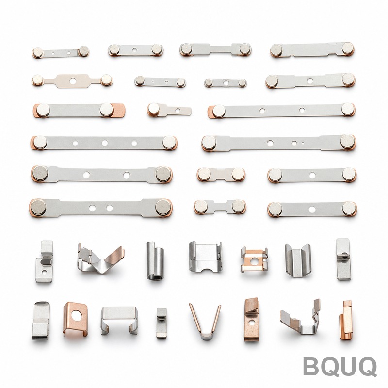
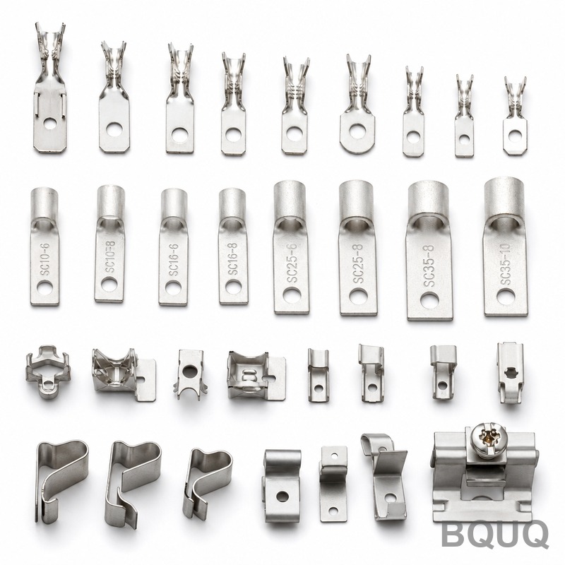
The part itself is not large. It is stamped from 0.8mm T2 copper strip, tin-plated, with a pierce-through lance, a formed spring wing, and tight cut-edge requirements. But every one of those features is electrical: the lance edge sets the wire contact, the spring wing sets the retention force, and the cut-edge quality sets the current path. Holding ±0.02mm on a 0.8mm strip, batch after batch, at volumes of 500,000 to 1,500,000 pieces per month, is where the real work is.
BQUQ Process Solution
The solution we proposed combined a dedicated progressive die, a controlled strip specification, and a plating process matched to the formed geometry - three decisions made together rather than separately.
Progressive Die and Strip Progression Design
We engineered a multi-station progressive die that carries the part through pierce, lance-and-form, spring-wing coining, and final blanking in one continuous strip. The strip progression keeps every feature referenced to the same datum from the first hit to the last, which is what holds hole-to-lance positions inside ±0.02mm without re-clamping variation. The spring wing is coined before final blanking so the work-hardened copper keeps its memory - the retention force stays where it was tuned instead of relaxing after the customer crimps the box.
Material and Contact Resistance Control
Contact resistance consistency starts with the strip, not the die. We locked the T2 copper specification with the mill: fixed temper, fixed grain direction relative to the progression, and incoming certificate checks on conductivity. On the die side, the lance pierce station uses a sharpening-interval discipline tied to cut-edge quality under a profile projector, not to a calendar. The result is a lance edge that produces the same biting geometry - and therefore the same contact resistance distribution - whether the part was stamped on day one of a die overhaul or day fifty.
Tin Plating Engineered for Formed Areas
Plating after forming, rather than before, was the decisive choice. Pre-plated strip loses coating thickness wherever the metal stretches - exactly at the formed shoulders where current concentrates. We stamp in bare copper, form, deburr, clean, and then apply electroplated tin at 3-5μm, with thickness verified on the formed features themselves. A post-plate passivation step protects the surface through packaging, ocean freight to India, and the customer's own storage window. Because plating is a separate gate in the flow, every lot also gets a solderability sample check before release, so the customer's wire-bonding and crimping operations downstream never inherit a surface problem discovered late.
Key Specifications
| Item | Specification |
|---|---|
| Material | T2 copper (C1100 equivalent), mill-certified strip |
| Strip thickness | 0.8mm ±0.02mm |
| Process | Progressive die stamping: pierce, lance, coining, form, blank |
| Surface finish | Electroplated tin 3-5μm on formed and flat areas, post-plate passivation |
| Critical tolerances | Feature positions ±0.02mm; burr height ≤0.05mm |
| Electrical requirement | Contact resistance consistency controlled batch-to-batch; every lot tested |
| Volume | 500,000 - 1,500,000 pcs/month |
| Inspection | First-article layout, profile projector checks at set intervals, per-lot contact resistance testing, CPK≥1.33 on critical dimensions |
| Delivery | Samples in 5-7 days after drawing approval, first mass batch in 15 days, then rolling monthly schedules |
Quality Control & Delivery
Every production run opens with a full first-article layout verified against the drawing. During the run, cut edges and formed shoulders are pulled on a fixed schedule and checked under a profile projector, and the plating line records thickness readings taken directly on the formed features. Critical dimensions are tracked statistically with CPK≥1.33 as the release criterion, all inside an ISO9001:2015 quality system, and every shipment leaves with a dimensional report and plating thickness data.
The outcome for the customer: contact resistance distribution tightened to the point that junction box final testing moved from screening mode to sampling mode, plating-related exposed-copper rejections dropped to effectively zero, and monthly volumes scaled smoothly from 500K toward 1.5M pieces as their module capacity expanded. Orders are scheduled on rolling monthly releases, so peak-season module campaigns no longer turn into supply emergencies.
Related Products & Resources
To see more parts in this category and how we produce them at scale, browse the Stamped Electrical Terminals & Contacts collection, or these related pages:
For our quality system, capacity planning and one-factory multi-process setup, visit About BQUQ.
FAQ
How consistent is the contact resistance between batches?
Every lot is tested before shipment, and the process holds a stable resistance distribution batch-to-batch by controlling the lance edge geometry, strip temper and plating thickness on formed areas. Critical dimensions run at CPK≥1.33, so the customer tests by sampling instead of screening every junction box.
Why plate after forming instead of using pre-plated strip?
Pre-plated 0.8mm strip thins out to below 2μm on stretched formed shoulders, exactly where current density is highest. Post-form plating puts the full 3-5μm on the shoulders as well as the flat areas, and we verify thickness on the formed features themselves, not just on coupons.
Can you support our volume of over 1 million pieces per month?
Yes. Our stamping lines run 100K to 5M pieces per month, and this program operates at 500K-1.5M pcs/month on rolling monthly releases. The progressive die design and the plating capacity were both sized with headroom so peak module season does not create a supply bottleneck.
What is the typical lead time for a new terminal program?
Standard samples ship 3-7 days after drawing approval for existing material; first mass batches land in 12-20 days including tooling trials and first-article approval. For this program, samples took 7 days including the plating process validation, and the first 500K-piece batch shipped within 15 days.