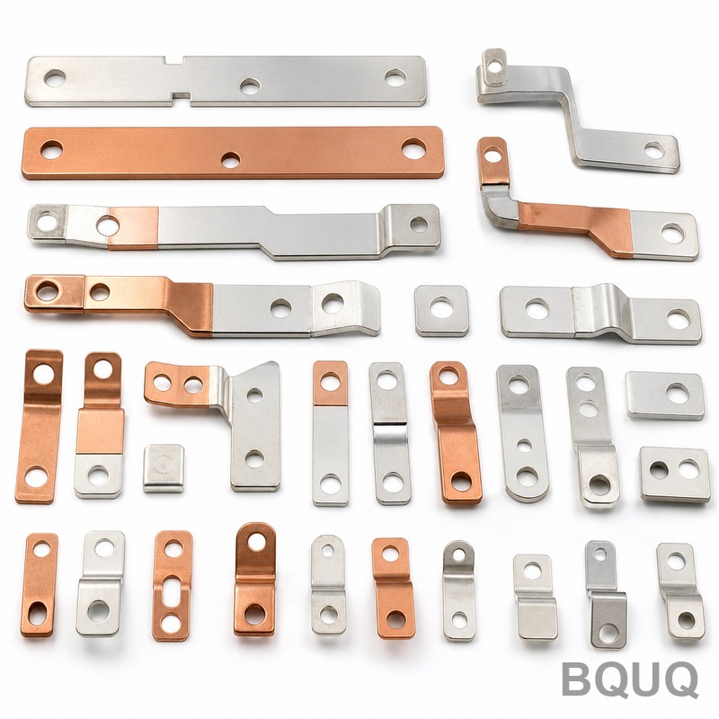
EV Battery Module Connector Plate Stamping: 1060 Aluminum, 0.8mm, Nickel-Plated
An EV battery module connector plate looks trivial on a drawing - a flat strip of aluminum with a few holes and a couple of forms. In production it is one of the least forgiving parts in the pack. At 0.8mm the aluminum has almost no stiffness of its own, and the moment nickel plating enters the process, flatness rather than profile becomes the specification that decides whether the part is accepted.
Project Background & Challenge
A Tier-1 EV battery module supplier in East China brought us a connector plate that ties individual cell tabs into a module-level busbar. Their previous source could produce the geometry but could not hold flatness after nickel plating. Parts that measured inside tolerance at the press came back from the plating line bowed by up to 0.3mm, and the assembly robots on the module line rejected them. Rework was manual, slow and never fully reliable.
The part is 1060 aluminum, 0.8mm thick - a high-conductivity, highly ductile grade that is ideal for a current-carrying connector but has almost no spring-back resistance and marks at the slightest contact. The drawing calls for hole positions within ±0.05mm, overall flatness of 0.1mm per 100mm after plating, a burr-free cut edge, and a matte nickel finish for corrosion resistance and stable contact resistance.
Those four requirements pull against each other. The stamping that forms the part introduces stress; the deburring that cleans the edge can reintroduce it; the plating bath that protects the surface adds heat and hydrogen that release whatever stress is left. Volume closed the door on soft options: the customer needed 200,000 pieces a month, ramping to 250,000 at model launch, which rules out any manual or semi-automatic route. The process had to be a continuous stamping line with in-line control, feeding a reel-to-reel plating line rather than batch barrel plating.
Flatness is not cosmetic on this part. A bowed connector plate changes the contact area between plate and cell tab, which raises joint resistance and can produce an uneven weld or a gap that the module tester flags. The 0.1mm flatness figure was written into the spec after a field issue, so there was no room to negotiate it down, and the customer wanted a source that could hold it by process rather than by sorting good parts from bad.
BQUQ Process Solution
Our approach was to treat flatness as a process variable from coil to shipping reel, not as a result inspected at the very end.
Die & Coil Preparation
A progressive die with a station sequence designed to keep the material as close to its neutral axis as possible. Instead of one heavy forming station that concentrates stress, forming is split into gentle incremental stages, and pilot holes are reused as datum references at every station so cumulative positioning error never builds. Incoming 1060 coil is checked for hardness and camber; cambered coil feeds a bowed strip into even a perfect die, so out-of-spec coils are rejected before they reach the press. Coil is also run through a straightener and loop control so the strip enters the first station at consistent tension; uneven entry tension is a quiet source of flatness variation that no amount of end-of-line inspection can recover.
Stamping & Deburring
Stamping runs on a continuous line at a controlled stroke rate, with in-die countersinks at the hole exits and die clearance set to shear cleanly rather than tear. Deburring is integrated into the tool rather than done later in a tumbler, which would knock the strip out of flat. Edges come off the press inside a 0.05mm burr limit, with flatness inside 0.05mm per 100mm before plating. Cutter geometry is matched to the ductility of 1060 so the shear face is smooth and the break face short, which keeps the edge inside that burr limit without a secondary operation.
Reel-to-Reel Nickel Plating
Parts stay on the carrier strip through a reel-to-reel plating line. Plating the strip in tension, instead of plating loose parts in a barrel, holds each plate flat through the bath. Nickel thickness is held at 1.5-3µm and controlled by current density and line speed; low-stress nickel chemistry and a controlled rinse sequence prevent hydrogen-driven distortion. Flatness is verified on the reel, not on a sample table. Bath chemistry and conductance are logged daily, because a drifting bath is the most common cause of a flat part leaving the line bowed.
Key Specifications
| Item | Specification |
|---|---|
| Material | 1060 aluminum, 0.8mm coil |
| Hole position | ±0.05mm |
| Flatness | 0.05mm/100mm pre-plate, 0.1mm/100mm after plating |
| Burr height | ≤0.05mm, deburred in-die |
| Surface finish | Reel-to-reel matte nickel, 1.5-3µm |
| Volume | 200,000 pcs/month, ramping to 250,000, no MOQ pressure |
| Inspection | In-die sensors + SPC, CMM first article, CPK≥1.33 |
| Delivery | First article 5 days, first production batch 18 days |
Quality Control & Delivery
First-article inspection is a full CMM layout plus a plated flatness check before the die is released to production. On the line, in-die sensors monitor feed position and tonnage, while hole position and flatness are charted with SPC so any drift is caught at the station rather than at final. CPK≥1.33 is maintained on hole position and flatness, and every shipment carries an inspection report with the CPK data, all under an ISO9001:2015 system.
Results: samples 5 days after drawing approval, the first 200,000-piece batch in 18 days, then monthly rolling schedules. Plated flatness settled at 0.06-0.08mm per 100mm, comfortably inside the 0.1mm limit, and the module line rejection rate fell from roughly 4% to under 0.2%. The line now holds about 250,000 pcs/month at peak without added tooling.
Related Products & Resources
This connector plate belongs to the wider family of stamped energy parts we build. See how the same continuous-die discipline is applied across related products:
A close relative in phosphor bronze, where contact resistance and spring properties matter more than conductivity, is covered in our case study on EV High Voltage Connector Terminal Stamping. More manufacturing questions are answered in our FAQ Center.
FAQ
Why does nickel plating distort a stamped aluminum part?
Two effects stack. Forming leaves residual stress in 0.8mm aluminum, and the plating bath adds heat and hydrogen that release it, which is what bowed the previous supplier's parts by up to 0.3mm. Plating on the carrier strip in tension instead of loose in a barrel keeps the part restrained through the bath, holding flatness to 0.06-0.08mm per 100mm.
What flatness can you actually hold after plating?
We hold 0.1mm per 100mm after nickel plating as the contractual limit, and in practice run 0.06-0.08mm per 100mm. Flatness before plating is held inside 0.05mm per 100mm, which gives us margin rather than relying on the plating line to fix a bowed strip. Hole position is held to ±0.05mm, and both features are charted with SPC at CPK≥1.33.
Can you really deliver 200,000 pieces a month?
Yes. The part runs on a continuous progressive die, which is why the volume was never the constraint - flatness was. First article ships in 5 days, the first full batch in 18 days, and the line sustains 200,000 to 250,000 pcs/month on rolling schedules with no MOQ pressure.
How do you control burrs without a tumbling operation?
Deburring is built into the die. In-die countersinks at the hole exits and controlled die clearance shear cleanly instead of tearing, so parts leave the press inside a 0.05mm burr limit. Tumbling would be faster on paper but would knock a 0.8mm aluminum strip out of flat, so we avoid it entirely. That is also why flatness is checked before plating as well as after, so a deburring problem never hides behind the nickel.