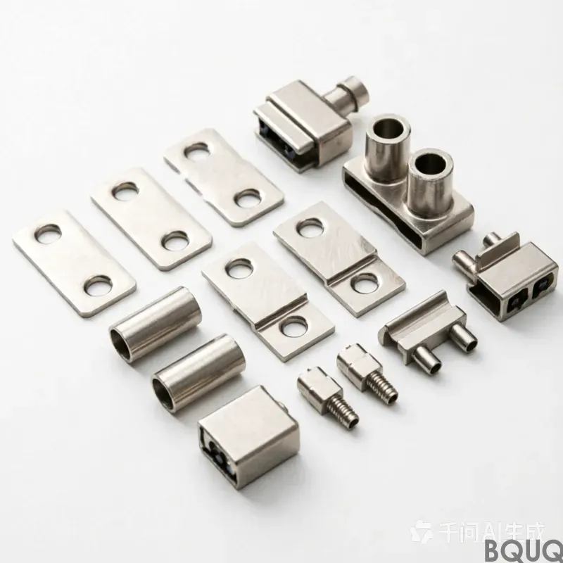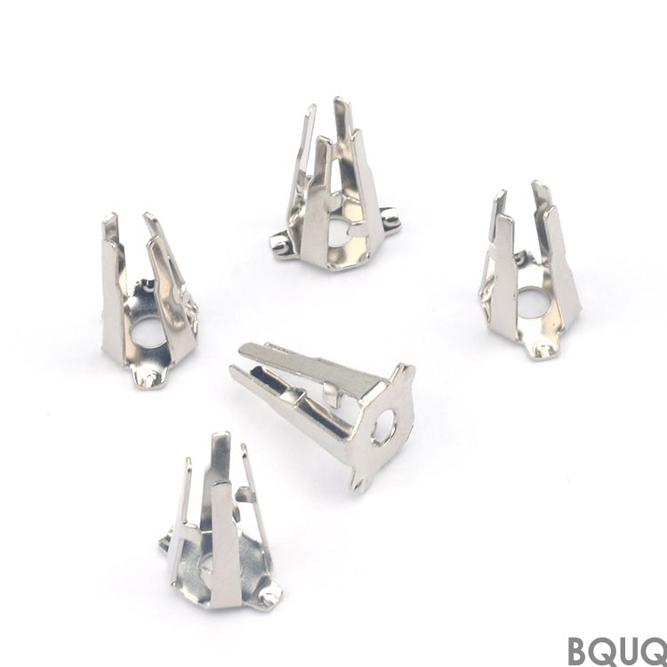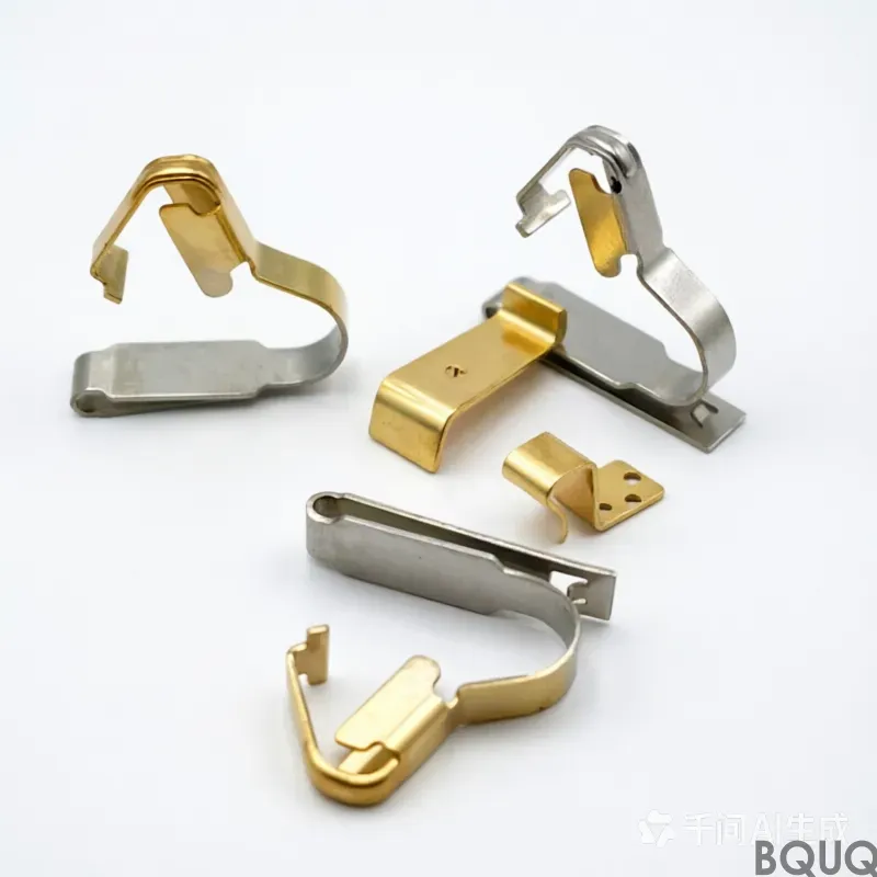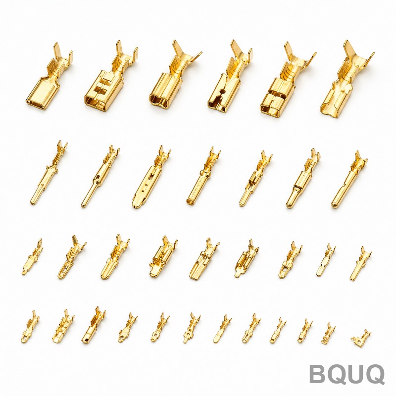
How Does 5G Connector Stamping Meet Telecom Precision Demands?
The direct answer is that 5G connector stamping meets telecom precision demands through ultra-tight tolerances of ±0.01 mm, specialized high-conductivity copper alloys, and progressive die technology operating at speeds up to 600 strokes per minute. This manufacturing process delivers the consistent, high-volume production required for millimeter-wave (mmWave) frequencies, where signal integrity is directly tied to dimensional accuracy and surface finish. For a 20-year veteran factory like BQUQ, mastering this niche means combining material science with micron-level tooling control to produce billions of interconnect components annually.
Why Is Precision Critical in 5G Connector Stamping?
The shift from 4G to 5G introduces operating frequencies from 3.5 GHz to 39 GHz, with some mmWave bands reaching 60 GHz. At these frequencies, the wavelength shrinks to between 5 mm and 8.6 mm, meaning any dimensional deviation in a stamped connector creates impedance mismatches, signal reflection, and insertion loss. A stamped contact with a tolerance of ±0.05 mm at 28 GHz can cause a voltage standing wave ratio (VSWR) degradation of up to 1.5:1, which is unacceptable for base station antennas and small cell backhaul modules.
Precision in 5G connector stamping is not only about the final part dimension but also about the consistency of the stamping process. Telecom OEMs such as Huawei, Ericsson, and Nokia require a Cpk (Process Capability Index) of 1.67 or higher on critical dimensions, meaning only 0.57 parts per million are allowed to fall outside specification. This forces stampers to control springback, material thickness variation, and tool wear in real-time, often using in-die sensors and servo-driven presses with feedback loops that adjust ram position every 5 milliseconds.
What Material Grades Are Used for 5G Stamped Connectors?
The choice of material directly affects the electrical performance and mechanical durability of 5G connectors. The most common base materials are beryllium copper (C17200), phosphor bronze (C52100), and high-performance brass (C26000), each selected for specific application requirements.
Beryllium copper is preferred for spring contacts in board-to-board and RF connectors because it retains its elastic modulus (131 GPa) after repeated deflection, resisting stress relaxation at temperatures up to 150°C. For high-frequency signal pins, phosphor bronze offers a good balance of conductivity (15% IACS) and formability, while brass is used for lower-cost shielding cans and grounding clips where conductivity matters less. A critical specification is the temper: for 5G applications, we typically specify C17200 in half-hard (HH) temper with a tensile strength of 620-790 MPa and a hardness of HV 300-360.
The plating system is equally critical. For 5G connectors exposed to outdoor environments, we recommend a base layer of 1.27-2.54 µm nickel followed by 0.76-1.52 µm of gold over the contact area. This ensures a contact resistance below 10 mΩ and prevents intermetallic growth that would degrade high-frequency performance. For cost-sensitive internal connectors, selective silver plating with a minimum thickness of 2.5 µm on the mating surface provides adequate performance up to 6 GHz.
How Does Progressive Die Design Affect Signal Integrity?
Progressive die design is the backbone of 5G connector stamping, converting a metal strip into a finished connector in a single pass through 20 to 40 stations. Each station performs a specific operation: piloting, coining, bending, forming, and cutting-off. The distance between stations, known as the feed pitch, is typically 20 mm to 50 mm, and the die must maintain a flatness of 0.005 mm across the entire working area to avoid stress concentrations that cause micro-cracks.
The critical factor for signal integrity is the control of the bend radius. For 5G connectors, the inside bend radius must be no less than 0.5 times the material thickness to prevent grain structure fractures that increase electrical resistance. For a 0.2 mm thick beryllium copper strip, the minimum bend radius is 0.1 mm, and we hold this dimension to ±0.005 mm using wire-cut EDM (Electrical Discharge Machining) die inserts with a surface finish of Ra 0.2 µm.
Another critical parameter is the burr height on the cut-off edge. A burr exceeding 0.03 mm on a signal contact creates a sharp point that concentrates electric fields, leading to corona discharge and passive intermodulation (PIM) at high power levels. To mitigate this, we employ fine-blanking technology on the final cut, achieving a burnish band of 100% of the material thickness and a burr height below 0.01 mm. The die is manufactured from powder metallurgy high-speed steel (e.g., ASP 2030) with a hardness of HRC 64-66 and coated with TiAlN (Titanium Aluminum Nitride) to extend tool life beyond 2 million strokes between regrinds.
What Tolerances Can Be Achieved in Production?
In high-volume production, 5G connector stamping can consistently hold tolerances that are tighter than general stamping by a factor of 5 to 10. For critical RF dimensions, we achieve a tolerance of ±0.01 mm, while non-critical mounting features can be held to ±0.05 mm. The flatness of the stamped part, especially for surface-mount (SMT) connectors, is maintained within 0.02 mm across the entire footprint.
The table below summarizes typical achievable tolerances for 5G connector stamping compared to standard stamping processes.
| Parameter | 5G Stamping Critical | 5G Stamping General | Standard Stamping |
| Dimensional tolerance (mm) | ±0.01 | ±0.03 | ±0.10 |
| Hole position tolerance (mm) | ±0.015 | ±0.05 | ±0.15 |
| Burr height (mm) | 0.01 max | 0.03 max | 0.10 max |
| Flatness (mm/25mm) | 0.02 | 0.05 | 0.15 |
| Surface roughness (Ra µm) | 0.4 | 0.8 | 1.6 |
| Bend angle accuracy (degrees) | ±0.5 | ±1.0 | ±2.0 |
| Cpk on critical dims | 1.67+ | 1.33+ | 1.00 |
To achieve these tolerances, the stamping press must be a high-precision servo press with a rigidity of at least 15 tons per millimeter of deflection. We utilize AIDA or Bruderer presses with a capacity of 80 to 250 tons, operating at speeds of 100 to 400 spm (strokes per minute) for 5G parts, compared to 600 spm for simpler components. The material strip is fed through a servo roll feeder with an accuracy of ±0.005 mm, ensuring that the pilot holes align perfectly with the die stations.
When Should You Choose Stamping Over CNC Machining for 5G Parts?
The decision between stamping and CNC machining for 5G connector components depends on volume, geometry, and cost per part. Stamping is the only economically viable option when the annual volume exceeds 1 million pieces per year, which is typical for mass-market 5G smartphones and base station arrays. The tooling investment for a progressive die ranges from $15,000 to $80,000, but the per-part cost drops to $0.02 to $0.15, depending on material and complexity.
CNC machining should be reserved for prototypes, low-volume production (under 50,000 parts per year), or geometries that cannot be formed in a die, such as internal threads or undercuts. For a simple RF contact pin, a CNC-machined part might cost $1.50 each, while a stamped part costs $0.05 each at volume. However, the lead time for a progressive die is 6 to 10 weeks, whereas CNC machining can deliver parts in 5 to 7 days.
A hybrid approach is often the most practical: use CNC machining for initial field trials and system integration, then transition to stamping once the design is frozen and volumes ramp. At BQUQ, we recommend this path to avoid the cost of die modifications during the early design iteration phase, which can add $2,000 to $5,000 per engineering change order (ECO) to the tooling budget.
How Does Thermal Management Affect Stamped Connector Design?
5G base stations generate significant heat, with power amplifiers (PAs) operating at junction temperatures up to 125°C. The stamped connectors must maintain electrical contact and mechanical integrity across a temperature range of -40°C to +105°C for outdoor equipment. Thermal expansion coefficients differ between the copper alloy (17 ppm/°C) and the PCB (14 ppm/°C for FR4), creating stress at the solder joint that can cause micro-cracks.
To manage this, we design stamped connectors with built-in stress-relief features, such as S-shaped beam contacts that absorb differential expansion without losing normal force. The contact normal force must be maintained between 50 and 150 grams-force (gf) over the entire temperature range. Below 50 gf, the contact resistance increases exponentially due to film formation; above 150 gf, the mating force becomes too high for multiple insertion cycles.
The material temper also plays a role. We specify beryllium copper in the mill-hardened condition (e.g., C17200 TH04) for applications above 85°C, as this temper provides the highest stress relaxation resistance. In accelerated life testing, a mill-hardened contact retains 90% of its initial normal force after 1,000 hours at 150°C, whereas a half-hard temper retains only 70%. This difference is critical for 5G equipment with a 15-year service life.
Can Stamped Connectors Handle High-Frequency mmWave Signals?
Yes, stamped connectors can handle mmWave frequencies, but only with careful attention to the transition zone between the stamped sheet metal and the PCB trace. At 28 GHz, the skin depth in copper is approximately 0.39 µm, meaning the signal travels only on the surface of the conductor. Therefore, the surface finish of the stamped part, especially on the contact face, must be better than Ra 0.4 µm to minimize conductor loss.
The geometry of the stamped contact must also mimic a coplanar waveguide (CPW) structure to maintain a controlled impedance of 50 ohms. The width of the signal trace and the gap to the ground plane must be held to ±0.02 mm to keep the impedance variation below 5%. This is achievable with our precision stamping process, but it requires a die design that accounts for the natural springback of the material, which can be up to 2 degrees for a 90-degree bend.
For the highest frequency bands (39 GHz and above), we recommend a stamped contact with a full-radius tip (e.g., 0.05 mm radius) to avoid sharp edges that radiate energy. Additionally, the mating interface must have a wipe length of at least 0.5 mm to break through any surface oxides and ensure a clean metallic contact. Our testing at BQUQ has shown that a properly designed stamped connector achieves an insertion loss of less than 0.1 dB per connector at 28 GHz and a return loss of better than -20 dB, which meets the requirements of 3GPP Release 15 specifications.
FAQ
What Is the Typical Lead Time for 5G Connector Stamping Tooling?
The lead time for a progressive die for a 5G connector ranges from 6 to 10 weeks, depending on the number of stations and the complexity of the geometry. A simple two-terminal connector with 15 stations takes about 6 weeks, while a complex 40-station die for a multi-pin RF connector can take 10 weeks. We recommend starting the tooling design review at least 2 weeks before the final CAD freeze to identify potential formability issues early.
How Much Does a 5G Connector Stamping Die Cost?
A progressive die for a 5G connector costs between $15,000 and $80,000, with the average being around $35,000 for a 20-station die. The cost is driven by the number of stations, the type of die steel (powder metallurgy vs. conventional), and the required tolerances. For instance, adding fine-blanking capability or in-die sensing increases the cost by 20% to 30%.
Which Material Is Best for High-Temperature 5G Applications?
Beryllium copper C17200 in the mill-hardened temper (TH04) is the best material for high-temperature 5G applications due to its superior stress relaxation resistance and thermal conductivity of 105 W/m·K. It can maintain 90% of its initial contact force after 1,000 hours at 150°C. Alternative materials like titanium copper (C19900) offer even higher strength but at a 20% cost premium.
Can You Stamp Connectors With 0.1 mm Wall Thickness?
Yes, we can stamp connectors with a wall thickness down to 0.05 mm, but the practical minimum for 5G RF connectors is 0.1 mm. Below this thickness, the material becomes difficult to handle in a progressive die, and the risk of tearing increases significantly. For very thin walls, we recommend using a material with high ductility, such as phosphor bronze in the soft temper, and reducing the stamping speed to 150 spm to minimize vibration.
What Inspection Methods Are Used to Verify 5G Stamping Quality?
We use a combination of in-line and off-line inspection methods for 5G stamped connectors. In-line, we use laser micrometers with a resolution of 0.1 µm to measure critical dimensions at 100% inspection rate. Off-line, we employ a coordinate measuring machine (CMM) with a resolution of 0.5 µm for full dimensional analysis, and a scanning electron microscope (SEM) for surface defect detection. Electrical testing includes a network analyzer to measure S-parameters up to 67 GHz on a sample basis.
How Do You Control Springback in 5G Connector Stamping?
Springback is controlled through a combination of over-bending, coining, and bottoming techniques in the die. We design the die with an over-bend angle of 1 to 3 degrees, then use a coining station to compress the material at the bend point, which reduces springback to near zero. For critical bend angles, we also add a bottoming station that applies additional pressure to set the final geometry.
What Is the Minimum Order Quantity for 5G Stamped Connectors?
The minimum order quantity (MOQ) for 5G stamped connectors is typically 100,000 pieces per part number for production parts. However, for initial qualification builds, we can provide 10,000 to 25,000 pieces using temporary tooling or a simplified die. The MOQ is primarily driven by the amortization of the tooling cost and the setup time of the press, which is about 2 hours per setup.
The precision demands of 5G connector stamping are met through a combination of advanced materials, high-tolerance progressive dies, and rigorous process control. At BQUQ, we have refined these techniques over 20 years of manufacturing experience, enabling us to deliver connectors that perform reliably at frequencies up to 67 GHz. If you are designing a 5G module or base station, we invite you to send your drawings for a feasibility review and a competitive quote within 12 hours. Contact us at sc@bquq.com or via WhatsApp at +86 13713157787, or visit our website at www.bquq.com to learn more about our precision stamping capabilities.