How Does Micro Stamping Meet Consumer Electronics Miniature Part Demand?
Micro stamping is the primary manufacturing process for producing miniature metal parts in consumer electronics, delivering precision components at tolerances down to ±0.01 mm with cycle times under one second per part. This high-speed, high-volume process uses progressive dies to stamp features like contacts, shields, and connectors from metal strips as thin as 0.05 mm, making it indispensable for smartphones, wearables, and IoT devices. For a factory like BQUQ with 20 years of experience, micro stamping offers the lowest cost-per-part for quantities above 100,000 units, often under $0.02 per piece, while maintaining repeatable accuracy across millions of cycles.
What Is Micro Stamping and Why Does Consumer Electronics Need It?
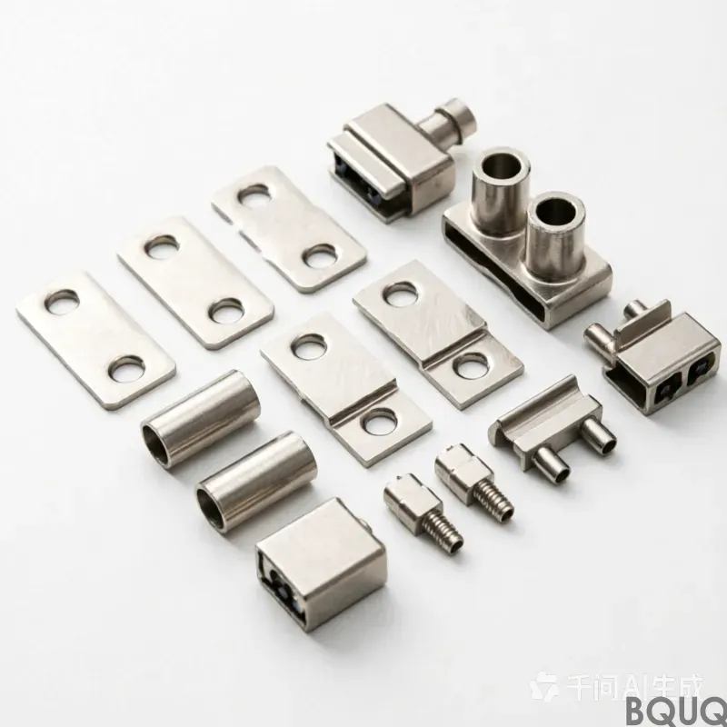
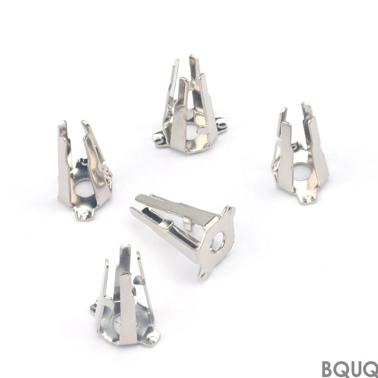
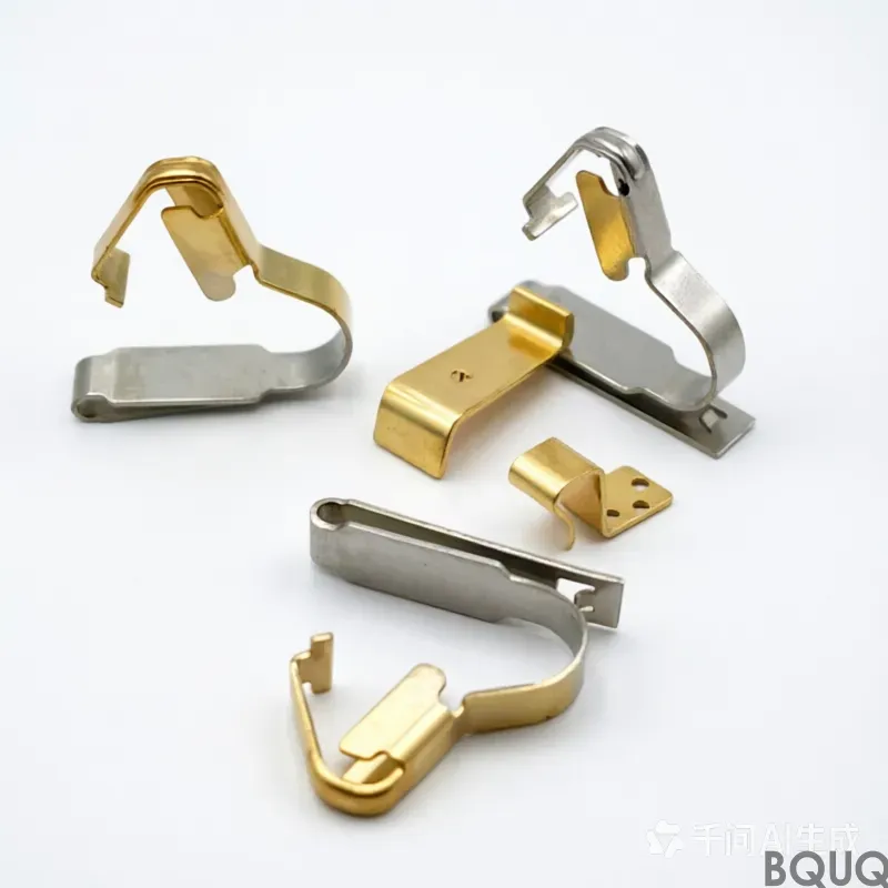
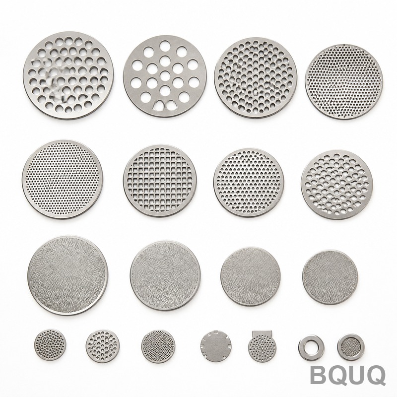
Micro stamping is a cold-forming process that uses precision dies and high-speed presses to cut, bend, and form metal features smaller than 5 mm in any dimension. In consumer electronics, components like SIM card ejector pins, battery contacts, EMI shielding frames, and camera module springs demand geometries that machining cannot produce economically at scale. The process works by feeding a continuous metal strip through a progressive die, where each station performs a specific operation—blanking, piercing, coining, or bending—until the finished part exits the final station. Typical production rates range from 300 to 1,200 parts per minute, which is why micro stamping dominates the supply chain for high-volume electronic devices.
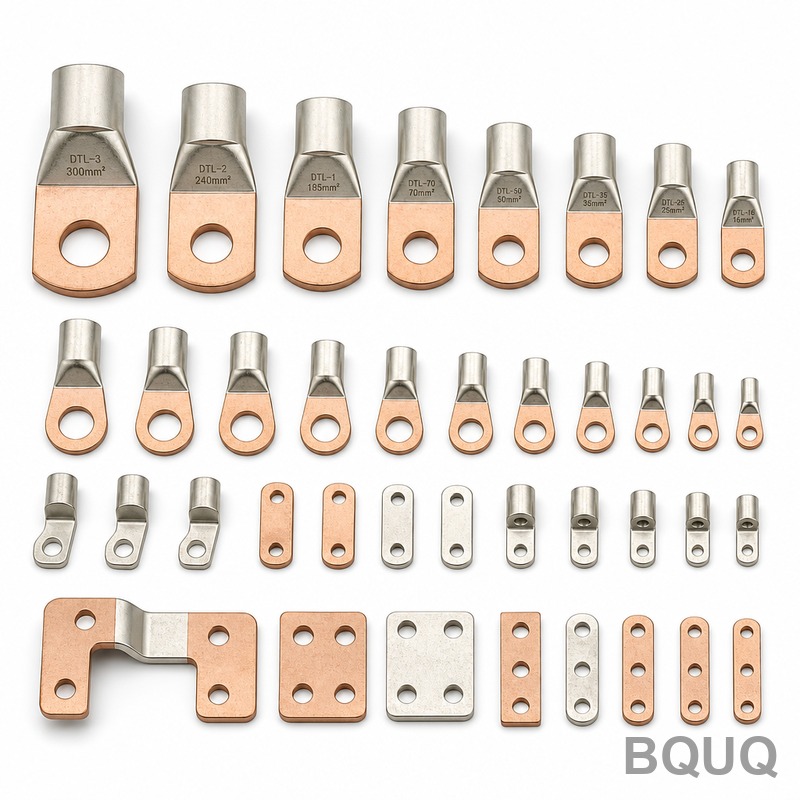
What Material Grades Are Best Suited for Micro Stamped Electronic Parts?
The most common materials for micro stamped consumer electronics parts are beryllium copper (C17200), phosphor bronze (C5210), stainless steel (301 and 304), and nickel-silver alloys. Beryllium copper offers the highest electrical conductivity (22% IACS) combined with a tensile strength of 1,200 MPa after heat treatment, making it ideal for spring contacts that must survive 500,000 deflection cycles. Phosphor bronze, at 50% IACS conductivity and 690 MPa tensile strength, is a lower-cost alternative for connectors and terminals where fatigue life is less critical. Stainless steel 301 is used for structural parts like SIM trays and shielding frames, providing corrosion resistance and a hardness of 480 HV in the full-hard temper. For battery contacts that operate at temperatures up to 85°C, nickel-silver (C75200) provides stable spring properties and a low contact resistance of 0.02 ohms.
How Tight Can Tolerances Be on Micro Stamped Components?
Micro stamping can hold dimensional tolerances of ±0.01 mm on critical features and ±0.025 mm on general dimensions, with positional accuracy of ±0.015 mm relative to the die reference point. The achievable tolerance depends on material thickness; for strips thinner than 0.10 mm, tolerances tighten to ±0.005 mm on hole diameters, while thicker materials above 0.30 mm allow ±0.02 mm. Surface finish on stamped edges ranges from Ra 0.8 µm to Ra 1.6 µm, which is sufficient for most electronic contact applications without secondary deburring. Flatness on stamped parts under 10 mm in length can be maintained at 0.03 mm maximum, critical for parts that must sit flush on printed circuit boards during reflow soldering.
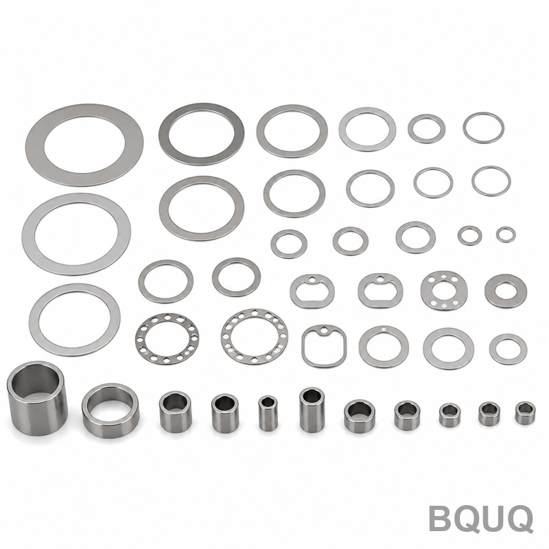
How Does Micro Stamping Cost Compare to CNC Machining and Etching?
For quantities above 100,000 pieces, micro stamping is 5 to 15 times cheaper per part than CNC machining and 2 to 3 times cheaper than chemical etching, primarily due to cycle time and material utilization. A typical micro stamped battery contact costs $0.015 to $0.04 per piece, whereas the same part machined from bar stock would cost $0.20 to $0.50 and require 30 seconds of machine time. Tooling investment for a progressive die ranges from $3,000 for a simple 4-station die to $25,000 for a complex 16-station die with in-die tapping and assembly. Chemical etching has a lower tooling cost at $500 to $1,500, but the per-part cost rises to $0.05 to $0.15 due to slower throughput and higher chemical waste disposal fees.
| Process | Min Quantity | Per-Part Cost | Tooling Cost | Lead Time (Tooling) | Tolerance |
| Micro Stamping | 100,000 | $0.015–$0.04 | $3,000–$25,000 | 3–6 weeks | ±0.01 mm |
| CNC Machining | 1 | $0.20–$0.50 | $0–$500 (fixture) | 1–2 weeks | ±0.005 mm |
| Chemical Etching | 500 | $0.05–$0.15 | $500–$1,500 | 1–2 weeks | ±0.02 mm |
| Laser Cutting | 100 | $0.10–$0.30 | $0–$1,000 | 3–5 days | ±0.05 mm |
Which Consumer Electronic Components Are Most Commonly Micro Stamped?
The highest-volume micro stamped components are spring contacts for battery and SIM card connections, followed by EMI shielding frames and camera module actuator springs. A single smartphone contains between 40 and 60 micro stamped parts, including the antenna contacts, charging port pins, speaker terminals, and vibration motor springs. Wearable devices like smartwatches add another 15 to 25 stamped parts, such as heart-rate sensor electrodes and haptic feedback springs. For true wireless earbuds, micro stamped charging contacts and latch springs are critical, with each earbud housing at least 8 stamped components that must withstand 10,000 insertion cycles. The medical device segment, including hearing aids and insulin pumps, uses micro stamped precision springs with wire diameters from 0.02 mm to 0.10 mm, requiring die clearances of 5% of material thickness.
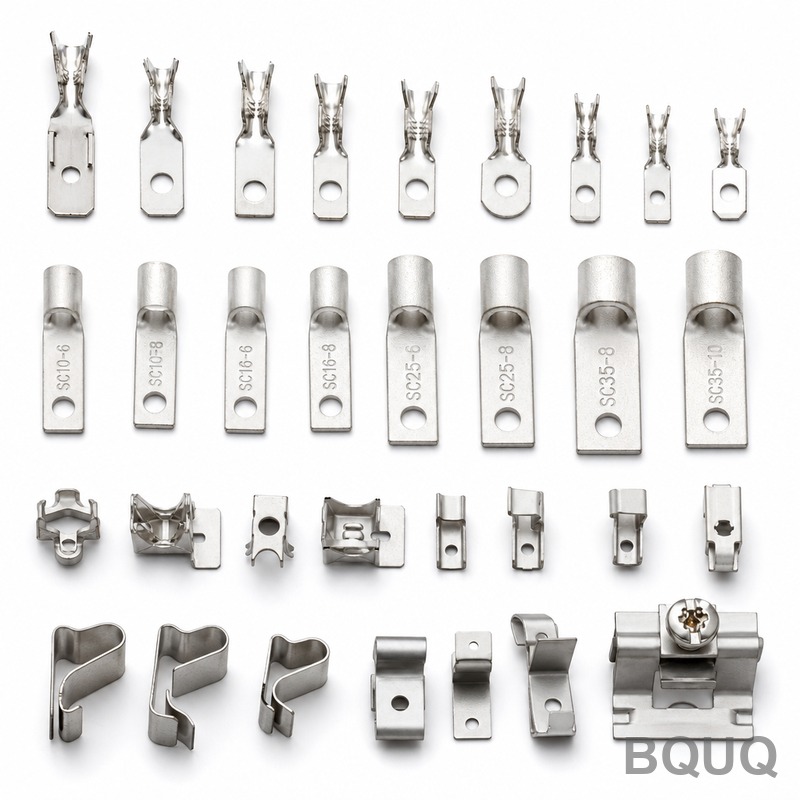
Why Does Tool Steel Selection Matter for Micro Stamping Die Life?
Die life in micro stamping is directly proportional to the hardness and wear resistance of the tool steel, with carbide dies lasting 5 to 10 times longer than high-speed steel dies. For production runs under 500,000 parts, D2 tool steel hardened to 58–60 HRC is cost-effective, providing 200,000 to 400,000 strokes before re-sharpening. For volumes above 1 million parts, tungsten carbide dies (90 HRA hardness) are mandatory, achieving 5 to 8 million strokes between regrinds. The clearance between punch and die must be precisely 4% to 8% of material thickness; for 0.10 mm thick stainless steel, this means a clearance of 0.004 mm to 0.008 mm per side. Maintaining a die surface finish of Ra 0.1 µm reduces friction and prevents galling on soft materials like copper alloys, extending die life by up to 30%.
How Do You Validate Quality in Micro Stamped Parts?
Quality validation for micro stamped parts uses a combination of optical measurement, coordinate measuring machines (CMM), and real-time process monitoring. Every production lot is sampled at 5% frequency using a vision system with a 0.001 mm resolution camera to check critical dimensions, burr height, and surface defects. Burr height on stamped parts must be controlled below 0.02 mm for electrical contacts, as excess burr causes arcing and premature failure. In-line force monitoring on the press detects tool wear by measuring stamping force variations; a 15% increase in force signals imminent die failure and triggers automatic machine stop. First article inspection reports include full dimensional data per IPC-A-600 standards, with Cpk values above 1.33 required for all critical characteristics before mass production begins.
What Are the Lead Times for Micro Stamping Tooling and Production?
A standard progressive die for micro stamping takes 3 to 6 weeks to design and manufacture, depending on the number of stations and complexity of the part geometry. Simple parts with 4 to 6 stations, like flat contacts, require 3 weeks, while complex parts with 12 to 16 stations, including forming, coining, and tapping operations, need 5 to 6 weeks. Once the die is approved, production lead time is 1 to 2 weeks for quantities up to 1 million parts, with daily output ranging from 200,000 to 500,000 parts per press. Prototype parts using soft tooling or wire EDM can be delivered in 3 to 5 days for design validation, but these parts do not reflect final stamped tolerances and should only be used for fit checks.
FAQ Section
How Do I Choose Between Micro Stamping and Metal Injection Molding?
Choose micro stamping for parts that are flat or bendable with thickness below 1.0 mm and require high electrical conductivity, as stamping preserves the material grain structure. Choose metal injection molding for parts with complex 3D shapes, undercuts, or thick walls above 1.5 mm, but accept a slower cycle time of 20–60 seconds per shot and higher per-part cost above $0.10.
Can Micro Stamping Handle Very Thin Materials Like 0.05 mm Copper?
Yes, micro stamping can process materials down to 0.03 mm thickness, but requires specialized dies with ultra-fine clearances and high-precision presses with minimal deflection. At 0.05 mm thickness, the die clearance must be 0.002 mm to 0.004 mm per side, and the press must maintain a ram position repeatability of ±0.005 mm to prevent tearing.
What Is the Maximum Part Size for Micro Stamping?
Micro stamping typically handles parts with a maximum footprint of 25 mm by 25 mm, though parts up to 50 mm are possible for simple flat geometries. Parts larger than 50 mm require a different class of precision stamping with larger presses and dies, which increases tooling costs by 40% to 60%.
How Do I Prevent Springback in Micro Stamped Bent Parts?
Springback compensation is achieved by over-bending the part by 2 to 5 degrees, with the exact value determined by material yield strength and bend radius. For stainless steel 301 full-hard, over-bend by 5 to 8 degrees; for beryllium copper, over-bend by 3 to 5 degrees. Using coining operations at the bend line, which compresses the material, can reduce springback by 80% compared to air bending.
What Is the Minimum Hole Size That Can Be Stamped?
The minimum hole diameter in micro stamping is 1.5 times the material thickness, so a 0.10 mm thick strip allows a minimum hole of 0.15 mm diameter. For holes smaller than this, laser micro-drilling or EDM must be used, adding $0.01 to $0.05 per hole in secondary cost.
How Does Part Cost Scale With Order Quantity?
Per-part cost drops significantly as quantity increases due to amortized tooling and setup costs. At 100,000 pieces, tooling adds $0.03 to $0.25 per part; at 1 million pieces, tooling cost drops to $0.003 to $0.025 per part, making the material cost the dominant factor.
What Finishes Are Applied to Micro Stamped Electronics Parts?
Common finishes include selective gold plating (0.1 to 0.5 µm) for contact surfaces, tin plating (2 to 5 µm) for solderability, and passivation for stainless steel parts. Gold plating costs $0.005 to $0.02 per part depending on surface area, while tin plating adds $0.002 to $0.008 per part.
Conclusion
Micro stamping is the most cost-effective and reliable method for producing miniature metal parts in consumer electronics, offering tolerances of ±0.01 mm, production rates up to 1,200 parts per minute, and per-part costs under $0.04 at volume. For engineers designing smartphones, wearables, or IoT devices, specifying micro stamped components with appropriate material selection and die design ensures consistent quality and manufacturability. BQUQ provides micro stamping services with in-house die design and manufacturing, supporting everything from prototype validation to high-volume production. For a quote within 12 hours, email your 2D or 3D drawings to sc@bquq.com, contact us on WhatsApp at +86 13713157787, or visit www.bquq.com.