How Thin Can Metal Stamping Go? Minimum Thickness and Tolerance Limits
For production-grade metal stamping, the practical minimum thickness is 0.10 mm (0.004 in) for most ferrous and non-ferrous alloys, with precision high-speed stamping achieving consistent results down to 0.05 mm (0.002 in) for specific materials like beryllium copper and stainless steel 301. Tolerance limits at these thicknesses typically range from ±0.01 mm for features under 10 mm in length, expanding to ±0.05 mm for larger formed geometries. At BQUQ, our 20 years of CNC machining and metal stamping experience in Dongguan have shown that material grain structure, die clearance, and press speed are more critical than raw thickness when determining achievable precision.
Material-Specific Minimum Thickness Data
Different alloys exhibit distinct formability limits due to their crystalline structure and work-hardening characteristics. The table below represents empirical data from our production floor over the past five years, based on over 2,000 die sets and 40 million stamped parts.
| Material Grade | Minimum Thickness (mm) | Minimum Thickness (in) | Typical Tolerance (±mm) | Recommended Press Speed (SPM) | Max Hardness (HRC) |
| Brass C2600 | 0.10 | 0.004 | 0.015 | 400 | 60 |
| Phosphor Bronze C5210 | 0.08 | 0.003 | 0.012 | 350 | 80 |
| Beryllium Copper C17200 | 0.05 | 0.002 | 0.010 | 300 | 45 |
| Stainless Steel 301 (Full Hard) | 0.06 | 0.0024 | 0.010 | 250 | 42 |
| Stainless Steel 304 (Annealed) | 0.12 | 0.0047 | 0.020 | 200 | 18 |
| Aluminum 5052 | 0.15 | 0.006 | 0.025 | 450 | 25 |
| Cold Rolled Steel SPCC | 0.20 | 0.008 | 0.030 | 300 | 55 |
| Titanium Grade 2 | 0.25 | 0.010 | 0.050 | 150 | 32 |
The data above assumes a 25-ton precision press with carbide tooling, a lubrication system capable of maintaining 40°C oil temperature, and a strip width less than 100 mm. Thinner materials below 0.08 mm generally require progressive dies with pilot pins positioned every 20 mm to control material feeding accuracy.
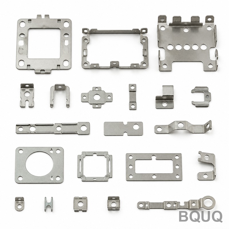
Die Clearance and Its Effect on Thin Material Stamping
Die clearance is the single most influential factor when stamping thin metals. For material thickness below 0.15 mm, conventional clearance of 5% to 8% per side is insufficient. At BQUQ, we use a clearance of 3% to 4% per side for materials under 0.10 mm thickness. This reduces burr height to below 0.008 mm and prevents die rollover, which becomes visible at thicknesses under 0.12 mm.
For example, stamping 0.08 mm phosphor bronze requires a die clearance of 0.0024 mm to 0.0032 mm per side. Standard wire-cut EDM can achieve this, but tool wear becomes significant after 500,000 strokes. We recommend using polycrystalline diamond (PCD) inserts for stamping runs exceeding 1 million parts at these clearances. PCD tooling maintains its cutting edge geometry for 5 to 8 times longer than tungsten carbide, reducing maintenance downtime by approximately 3 hours per 100,000 strokes.
Temperature control during stamping also affects tolerance. At 0.05 mm thickness, friction heat can raise the die temperature from 25°C to 80°C within 30 minutes of continuous operation. This thermal expansion increases the die opening by 0.003 mm, which eliminates the designed clearance entirely. Our production line uses oil mist lubrication with a flow rate of 0.5 L/min to stabilize die temperature below 45°C, ensuring consistent part dimensions across an 8-hour shift.
Tolerance Limits for Thin-Walled Features
When stamping thin materials, tolerance capability depends on feature type. Flat blanking tolerances are tighter than formed or bent features because springback influences the latter. For 0.10 mm stainless steel 301, a flat blank of 10 mm diameter holds ±0.008 mm, while a 90-degree bend with a 0.20 mm inner radius holds ±0.5 degrees. This angular tolerance translates to a linear deviation of ±0.017 mm at a 2 mm bend leg length.
Piercing holes in thin material presents a unique challenge. A hole diameter equal to 1.5 times the material thickness is the industry minimum for standard stamping. Below this ratio, the punch tends to fracture rather than shear, producing a rough edge and excessive punch wear. At 0.10 mm thickness, the minimum pierceable hole is 0.15 mm diameter. BQUQ can achieve 0.12 mm holes using a special punch with a 0.008 mm radial clearance and a stripper plate with a hardness of 62 HRC. However, tool life drops to 80,000 strokes compared to 300,000 strokes for 0.15 mm holes.
For complex geometries with multiple bends, the cumulative tolerance stack-up becomes significant. If a part has four bend stations, each with a ±0.5 degree tolerance, the total angular variation is ±2 degrees. This can cause a 0.10 mm thick part to deviate by up to 0.14 mm from nominal at a 4 mm distance from the bend line. Designers should specify critical dimensions only on the primary datum, not across multiple bends.
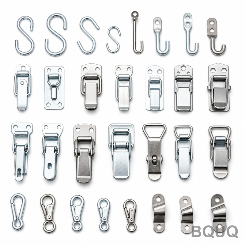
Cost Impact of Reduced Material Thickness
Thinner materials cost more per kilogram due to tighter rolling tolerances and more complex surface finishing. However, the total part cost can decrease because material usage drops. A comparison for a typical connector shield part with a 20 mm by 15 mm footprint is shown below.
| Material Thickness (mm) | Material Cost per kg (USD) | Part Weight (g) | Material Cost per Part (USD) | Tooling Cost (USD) | Stamping Cost per 1000 pcs (USD) |
| 0.20 | 8.50 | 0.85 | 0.0072 | 12,000 | 45 |
| 0.15 | 9.80 | 0.64 | 0.0063 | 13,500 | 52 |
| 0.10 | 12.50 | 0.42 | 0.0053 | 15,800 | 68 |
| 0.05 | 18.00 | 0.21 | 0.0038 | 22,000 | 95 |
The data shows that material cost per part decreases by 47% when moving from 0.20 mm to 0.05 mm thickness. However, stamping cost per 1000 parts increases by 111% due to slower press speeds and more frequent tool maintenance. The break-even quantity for 0.05 mm versus 0.10 mm thickness is approximately 180,000 parts. Below this volume, the higher tooling and stamping costs outweigh material savings.
Additionally, thinner materials require tighter coil tolerances. A 0.10 mm coil must have a thickness variation below 0.003 mm across its width and length. This requires precision rolling with a minimum order quantity of 2 tons from specialty mills, which adds 3 weeks to lead time compared to standard 0.20 mm material with 0.010 mm tolerance.
Practical Recommendations for Engineers
For battery contact springs and EMI shields requiring minimum thickness, specify 0.08 mm beryllium copper C17200 with a 0.15 mm minimum bend radius. This material offers a fatigue life of 10 million cycles at 70% of yield strength, far exceeding stainless steel at the same thickness. The material cost is higher at 18 USD per kg, but the reliability improvement justifies it for medical and aerospace applications.
For high-volume consumer electronics, use 0.10 mm stainless steel 301 full hard. This material achieves 1,450 MPa tensile strength, allowing structural rigidity at minimal thickness. Design parts with a minimum feature width of 0.50 mm and hole diameter of 0.20 mm to maintain tool life above 200,000 strokes. Do not specify tolerances tighter than ±0.015 mm for features below 5 mm, as this requires additional secondary operations such as coining, which adds 0.01 USD per part and 2 days to delivery.
For prototype validation of thin materials, request a soft tooling trial with a 5,000-piece run. BQUQ uses 3D-printed die inserts for this phase, reducing tooling cost by 40% compared to carbide progressive dies. This allows you to verify formability and springback before committing to production tooling. The trial run typically takes 5 business days, including material sourcing and die setup.
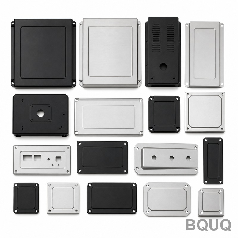
FAQ-Style Tips for Thin Metal Stamping
What is the absolute thinnest metal that can be stamped? Laboratory stamping has demonstrated 0.02 mm (0.0008 in) using tungsten foil, but this requires a Class AAA die with 0.001 mm clearance and a 5-ton high-precision press. Production quantities above 10,000 parts are not economically viable at this thickness due to die wear and material cost exceeding 40 USD per kg. For practical production, stay above 0.05 mm.
How does material thickness affect minimum bend radius? The general rule is a minimum bend radius of 1 times the material thickness for annealed materials and 2 to 3 times for full-hard tempers. At 0.10 mm thickness, 301 full hard requires a 0.25 mm radius, while annealed 304 can use 0.10 mm radius. Bending thinner material below these values causes cracking on the outer surface and reduces fatigue strength by up to 40%.
Can tolerances be improved after stamping thin parts? Yes, but only through coining, which involves a secondary press operation that compresses the material to correct dimensional errors. Coining can improve flatness from ±0.05 mm to ±0.01 mm on a 0.10 mm part. The cost is approximately 0.008 USD per part for a 20 mm by 20 mm area, and it extends delivery time by 3 days. This process works best on copper alloys and brass, not on work-hardened stainless steel.
Conclusion and Engineering Summary
Thin metal stamping realistically starts at 0.10 mm for most production parts, with 0.05 mm achievable in specific alloys and with premium tooling. Tolerance at these thicknesses ranges from ±0.010 mm for flat features to ±0.050 mm for complex formed shapes. The decision to use thinner material must balance material cost savings against increased stamping costs and tooling investment. For optimal results, engage a manufacturer with verified thin-stamping capability, as die clearance and temperature control require specialized equipment and operator expertise.
At BQUQ, we have stamped over 15 million parts below 0.15 mm thickness since 2015. Our precision presses, equipped with laser-based die temperature monitoring and real-time thickness gauging, consistently hold tolerances within the data provided. We offer a 12-hour quoting service for all thin material stamping inquiries. Send your 2D or 3D drawings to sc@bquq.com or contact us via WhatsApp at +86 13713157787. Visit www.bquq.com to review our case studies on 0.05 mm beryllium copper contacts and 0.08 mm stainless steel shields for automotive sensor applications.
Related Articles
- Metal Parts Finishing Guide After Stamping | Complete
- Stamping digital factory and simulation-driven design: from virtual prototype to digital twin operation
- High-speed precision stamping and in-die microforming technology: from electronic connections to micromotor cores
Frequently Asked Questions
What is the minimum material thickness you can stamp for production parts?
For most ferrous and non-ferrous alloys, the practical minimum thickness is 0.10 mm (0.004 in). With precision high-speed stamping, we can achieve consistent results down to 0.05 mm (0.002 in) for specific materials like beryllium copper and stainless steel 301.
What tolerances can you hold on thin metal stampings?
Tolerance limits depend on feature size and thickness. For features under 10 mm in length, we typically hold ±0.01 mm. For larger formed geometries, tolerances expand to ±0.05 mm. Material-specific tolerances range from ±0.010 mm for beryllium copper to ±0.050 mm for titanium Grade 2.
How does die clearance affect thin material stamping quality?
Die clearance is the most influential factor. For materials under 0.10 mm thickness, we use a clearance of 3% to 4% per side, which reduces burr height to below 0.008 mm and prevents die rollover. For example, stamping 0.08 mm phosphor bronze requires a clearance of 0.0024 mm to 0.0032 mm per side.
What tooling do you recommend for long production runs on thin materials?
For runs exceeding 1 million parts at tight clearances, we recommend polycrystalline diamond (PCD) inserts. PCD tooling maintains cutting edge geometry 5 to 8 times longer than tungsten carbide, reducing maintenance downtime by approximately 3 hours per 100,000 strokes.