Why Is Copper and Brass Stamping Demand Growing for Electrical Components?
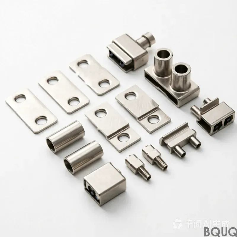
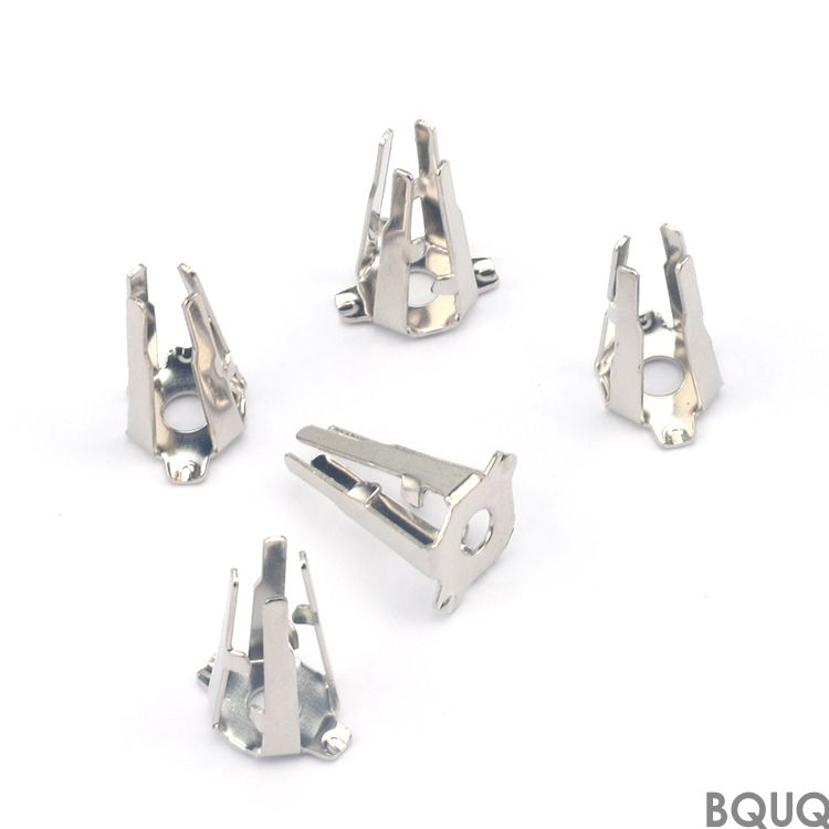
Copper and brass stamping demand for electrical components is growing because of the global push toward electrification, renewable energy infrastructure, and electric vehicles, which require highly conductive, corrosion-resistant metal parts at high volume. Copper offers 58.0 MS/m electrical conductivity (100% IACS), while brass provides a cost-effective alternative with 23-27% IACS conductivity plus superior spring properties for connectors and terminals. This growth is projected at 6.8% CAGR through 2030, driven by transformer production, EV battery interconnects, and 5G base station shielding.
What Are the Key Electrical Properties of Copper and Brass for Stamping?
Copper C11000 (electrolytic tough pitch) is the industry standard for electrical stampings, delivering 100% IACS conductivity with a tensile strength of 220-250 MPa in the annealed condition. Brass C26000 (cartridge brass, 70% copper, 30% zinc) offers 28% IACS conductivity but significantly higher tensile strength of 300-360 MPa, making it ideal for spring contacts and fuse clips where mechanical force is required. For high-temperature applications, beryllium copper C17200 provides 22% IACS conductivity with a remarkable 1,150-1,400 MPa tensile strength after heat treatment, though at a material cost premium of 8-12 times that of standard brass. When selecting materials, engineers must balance conductivity against mechanical strength, as yield strength in copper drops to 70 MPa when annealed for maximum conductivity, while brass maintains 200 MPa yield in the half-hard condition.
How Does Stamping Tolerance Affect Electrical Component Performance?
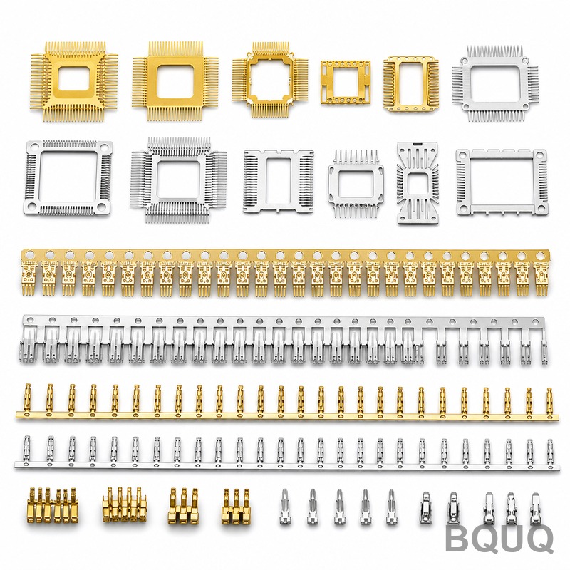
Precision stamping of copper and brass for electrical components achieves tolerances of plus/minus 0.025 mm for critical dimensions under 25 mm, and plus/minus 0.05 mm for features up to 100 mm. These tolerances are essential for connector pin alignment, where a 0.1 mm deviation can cause a 30% increase in contact resistance due to reduced mating surface area. Progressive die stamping maintains these tolerances at production speeds of 300-800 strokes per minute, with die steel hardness of 58-62 HRC ensuring 1-5 million hits before maintenance is required. For high-volume electrical terminals, BQUQ recommends designing with a minimum 0.3 mm material thickness and 0.5 mm bend radius to prevent cracking in copper's annealed grain structure, particularly when forming 90-degree bends for battery connectors.
Why Is Brass Preferred Over Copper for Spring Contacts and Terminals?
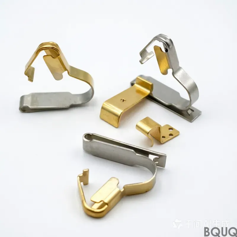
Brass C26000 in the spring temper (extra hard, 490-540 MPa tensile) is preferred for electrical spring contacts because it retains 85-90% of its yield strength after stamping, while copper loses 60-70% of its strength when formed to the same geometry. This mechanical resilience prevents contact fatigue in applications like relay blades and socket terminals that experience 10,000-100,000 insertion cycles. Brass also exhibits a lower coefficient of friction (0.35 vs 0.50 for copper) against steel mating surfaces, reducing insertion force in connectors by 25-40% and improving user experience in automotive and consumer electronics. However, for busbars and high-current power distribution (above 100 A), pure copper remains the only choice because brass's higher resistivity causes excessive I²R heating, with a 50% temperature rise at equivalent current density.
Which Stamping Process Is Most Cost-Effective for High-Volume Electrical Parts?
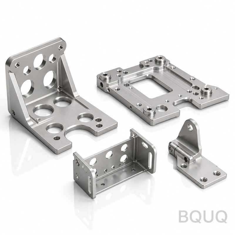
Progressive die stamping is the most cost-effective process for electrical components with production volumes above 100,000 parts per year, achieving piece prices of 0.005-0.05 USD depending on complexity and material thickness. Four-slide stamping (multi-slide) is superior for complex wire-formed contacts and terminals with multiple bends, offering 20-30% lower tooling cost than progressive dies for parts under 50 mm in length. For prototyping or low-volume production (under 5,000 pieces), CNC punching or laser cutting of copper and brass sheets is practical, with lead times of 3-5 days versus 4-6 weeks for hard tooling, but piece costs are 5-10 times higher. The table below summarizes typical cost and lead time benchmarks for copper and brass stamping processes.
| Process | Tooling Cost (USD) | Piece Cost (USD) | Lead Time (Weeks) | Min Volume | Tolerance (mm) |
| Progressive Die | 5,000 - 50,000 | 0.01 - 0.10 | 4 - 6 | 100,000/yr | plus/minus 0.025 |
| Four-Slide | 3,000 - 30,000 | 0.02 - 0.15 | 3 - 5 | 50,000/yr | plus/minus 0.050 |
| CNC Punching | 500 - 2,000 | 0.50 - 2.00 | 0.5 - 1 | 1 - 100 | plus/minus 0.100 |
| Laser Cutting | 0 - 500 | 1.00 - 3.00 | 0.5 - 1 | 1 - 50 | plus/minus 0.150 |
How Does Material Thickness Influence Stamping Design for Electrical Conductors?
Material thickness directly determines current-carrying capacity, with a 0.5 mm copper stamping carrying 15 A per 10 mm width, while a 1.0 mm thickness carries 30 A under the same 30-degree Celsius temperature rise condition. For brass, the same geometry carries only 8 A and 16 A respectively, due to its higher resistivity, meaning designers must increase cross-sectional area by 60-100% when substituting brass for copper. Thinner materials (0.1-0.3 mm) are suitable for EMI shielding gaskets and flexible connectors, where grain size must be controlled to ASTM 0.015-0.025 mm to prevent cracking during tight radius bending. BQUQ recommends specifying material thickness with a tolerance of plus/minus 0.03 mm for stamped copper parts, as thickness variation directly impacts contact force and electrical resistance in mating connectors.
What Surface Finishes Are Required for Copper and Brass Electrical Stampings?
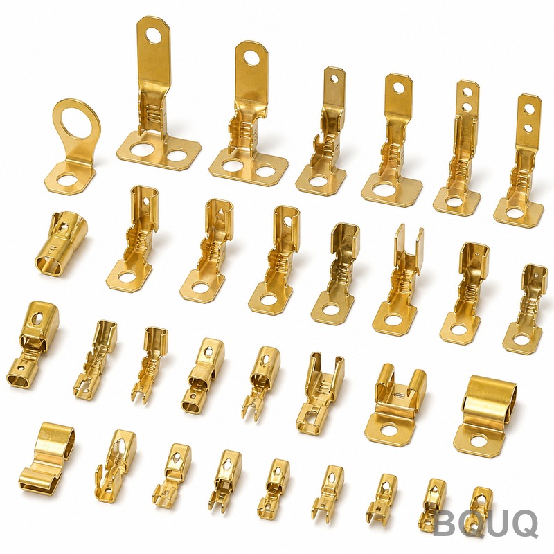
Bare copper and brass surfaces oxidize rapidly, increasing contact resistance by 200-400% within 6 months in humid environments, so most electrical stampings require protective finishes. Tin plating (2-5 micrometers) is the most common for copper busbars and terminals, maintaining low contact resistance up to 150 degrees Celsius and costing 15-25 USD per square meter. Silver plating (1-3 micrometers) is specified for high-frequency RF connectors and high-current switches, offering 5% better conductivity than tin but at 40-60 USD per square meter. For brass springs, a nickel underplate (1-2 micrometers) plus gold flash (0.1-0.5 micrometers) is typical for critical signal contacts in automotive and aerospace, though this adds 80-120 USD per square meter to the stamping cost. Selective plating, where only the contact area is plated, reduces material cost by 50-70% for parts longer than 20 mm and is recommended for high-volume production.
Can Copper and Brass Stamping Meet RoHS and REACH Compliance Requirements?
Yes, copper and brass stampings fully comply with RoHS (Restriction of Hazardous Substances) and REACH (Registration, Evaluation, Authorisation and Restriction of Chemicals) regulations when using lead-free brass alloys such as C27450 or C26000 with lead content below 0.1% by weight. Traditional free-machining brass C36000 contains 2.5-3.7% lead, which is prohibited in electrical components sold in the European Union, so BQUQ exclusively sources lead-free brass for all electrical stamping projects. Compliance documentation, including material test certificates per EN 10204 type 3.1 and XRF (X-ray fluorescence) test reports, is provided with every shipment to verify conformity. For applications requiring high-temperature operation above 200 degrees Celsius, cadmium-free copper alloys like C17200 beryllium copper are recommended, as they maintain mechanical properties without hazardous additives.
FAQ
What Is the Maximum Current Capacity of a Copper Stamping?
A 1.0 mm thick copper stamping with 10 mm width carries approximately 30 A continuous current at a 30-degree Celsius temperature rise above ambient. For higher currents, increase width proportionally or use multiple parallel stampings to distribute heat. Always verify with thermal simulation for duty cycles above 50% to prevent overheating.
How Long Does a Progressive Die Last for Copper Stamping?
A well-maintained progressive die using D2 or M2 tool steel (58-62 HRC) produces 3-8 million copper stampings before requiring re-sharpening. Brass, being less abrasive, extends die life to 5-10 million hits. BQUQ recommends scheduled maintenance every 500,000 strokes to maintain tolerances and surface finish.
What Is the Minimum Bend Radius for Brass Stamping?
The minimum bend radius for brass C26000 in half-hard condition is 0.5 times material thickness, while annealed copper requires 1.0 times thickness to prevent cracking. For spring temper brass, increase to 1.5 times thickness to avoid micro-fractures that reduce fatigue life. Bend lines should be perpendicular to the rolling direction for best formability.
Which Copper Alloy Is Best for High-Temperature Electrical Applications?
Beryllium copper C17200 is best for continuous operation up to 200 degrees Celsius, maintaining 75% of its room-temperature strength at this level. For up to 300 degrees Celsius, use copper-chromium alloy C18200 with 80% IACS conductivity and excellent resistance to stress relaxation. Standard copper C11000 is limited to 150 degrees Celsius for structural applications.
How Does Stamping Affect Electrical Conductivity of Copper?
Stamping cold-working reduces copper's conductivity by 2-5% due to increased dislocation density and grain distortion. For critical conductivity applications, specify annealed copper (O temper) after stamping or use a stress-relief anneal at 200-300 degrees Celsius for 1 hour. This restores conductivity to 98-100% IACS while maintaining acceptable strength.
What Is the Typical Lead Time for Custom Copper Stamping Tooling?
Standard progressive die tooling for copper and brass stampings takes 4-6 weeks from design approval to first article inspection. BQUQ offers expedited tooling at a 20-30% surcharge for 3-week delivery when using standardized die components. Design for manufacturability review adds 2-3 days but reduces tooling rework by 40% on average.
Can Brass Stampings Replace Copper in All Electrical Applications?
No, brass cannot replace copper for high-current applications above 50 A because its 28% IACS conductivity creates excessive heat and voltage drop. Brass is suitable for signal-level currents below 5 A, spring contacts, and mechanical connectors where spring force is required. For busbars, power terminals, and battery interconnects, copper remains mandatory.
Conclusion
The growing demand for copper and brass stampings in electrical components is driven by tangible engineering advantages: copper's unmatched conductivity for power distribution and brass's mechanical resilience for contact applications. By selecting the correct alloy, temper, and plating, and by partnering with an experienced stamper like BQUQ, you achieve reliable performance at 0.01-0.10 USD per part with tolerances of plus/minus 0.025 mm. BQUQ, with 20 years of precision manufacturing in Dongguan, China, offers complete in-house tooling, stamping, plating, and inspection, with 12-hour quoting for your drawings and prototypes.
For a fast, accurate quote on your copper or brass stamping project, contact BQUQ today. Email us at sc@bquq.com, reach us on WhatsApp at +86 13713157787, or visit www.bquq.com to upload your CAD files and receive pricing within 12 hours.