Electrical Contacts and Terminals: How Precision Stamping Ensures Long-Term Reliability
Precision stamping is the definitive manufacturing process for electrical contacts and terminals because it delivers micron-level dimensional repeatability, superior surface finish, and high-volume cost efficiency that alternative methods like machining or fabrication cannot match. By controlling material grain flow and maintaining tolerances as tight as ±0.01 mm, stamping ensures consistent contact pressure, minimal electrical resistance, and predictable thermal performance across millions of cycles. This article provides the engineering data and process parameters required to specify stamped contacts for mission-critical applications.
Material Selection and Plating: The Foundation of Contact Reliability
The base metal and plating system determine 80% of a contact's electrical and mechanical lifespan. For power applications, BQUQ recommends copper alloys such as C17200 beryllium copper (yield strength 1100–1300 MPa) or C52100 phosphor bronze (yield strength 450–600 MPa). For signal-level connectors, C19400 copper-iron (conductivity 60% IACS) offers a balance of strength and cost.
Plating is applied after stamping to preserve the spring properties of the base metal. Selective plating in gold (0.76–1.27 µm) or palladium-nickel (1.0–2.5 µm) is standard for automotive and industrial connectors. For high-temperature environments above 150°C, avoid tin plating due to oxidation; use silver (2.0–5.0 µm) or nickel underplating (1.27–2.54 µm). The surface roughness of the stamped contact area should be Ra 0.4 µm or better to minimize micro-arcing and fretting corrosion.
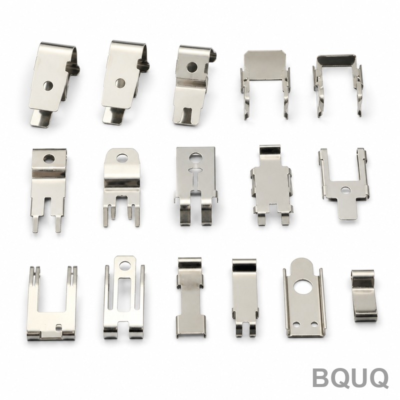
Precision Stamping Tolerances and Die Technology
A precision progressive die for contacts operates at 300–800 strokes per minute, producing parts with dimensional stability that is unattainable by manual assembly. Critical tolerances for stamped terminals are as follows:
- Pitch accuracy (center-to-center): ±0.02 mm over 50 positions - Flatness: 0.05 mm over a 25 mm length - Burr height: maximum 0.03 mm on cut edges, controlled by die clearance of 4–6% of material thickness - Edge radius: 0.05–0.10 mm for contact mating zones
The stamping die uses carbide inserts with a hardness of 88–92 HRA. Die life exceeds 10 million strokes before requiring re-grinding. For high-current terminals (above 50 A), consider coining operations within the same die to densify the material at the contact surface, reducing contact resistance by up to 15%.
Contact Resistance and Thermal Performance Data
The reliability of a stamped contact is quantified by its steady-state contact resistance, which must remain stable over the product lifetime. The table below shows typical values for different material and plating combinations tested at 10 A and 30 mV open-circuit voltage.
| Material and Plating | Contact Resistance (mΩ) | Max Continuous Current (A) | Operating Temperature (°C) | Insertion Force (N) | Durability Cycles |
| C17200 BeCu, Gold 0.76 µm | 5–8 | 5 | -55 to 125 | 1.5–3.0 | 10,000 |
| C52100 PhBr, Tin 3.0 µm | 12–18 | 3 | -40 to 105 | 2.0–4.0 | 500 |
| C19400 CuFe, Silver 2.5 µm | 8–12 | 15 | -55 to 200 | 3.5–5.5 | 1,000 |
| C17200 BeCu, PdNi 1.5 µm | 6–9 | 8 | -55 to 150 | 2.0–3.5 | 5,000 |
| Brass C26000, Selective Gold 1.27 µm | 10–15 | 2 | -40 to 85 | 1.0–2.0 | 200 |
For every 10°C rise above 85°C, the oxidation rate of unprotected copper doubles. Precision stamping minimizes this risk by producing a clean, work-hardened surface that accepts plating uniformly. The stamped edge grain structure must be oriented to prevent crack propagation under repeated bending, which is why the strip rolling direction is aligned with the contact beam axis.
Cost and Lead Time Comparison: Stamping vs. Machining
For production volumes above 50,000 pieces per year, precision stamping is the only economically viable process. The tooling investment for a progressive die ranges from $8,000 to $25,000 depending on the number of stations (typically 8–20). Unit costs fall below $0.05 for simple terminals and reach $0.30 for complex multi-bend contacts with selective plating.
Manual machining (CNC milling or turning) has no die cost but a unit cost of $1.50–$5.00 per piece, making it 30–50 times more expensive at scale. Machining also introduces residual stress and burrs that require secondary deburring, increasing lead time. Stamping lead time for prototypes is 5–7 days using soft tooling (aluminum die), while production tooling requires 15–20 days. In contrast, machined samples ship in 2–3 days but production lead times stretch to 4–6 weeks due to per-part machining hours.
| Process | Tooling Cost (USD) | Unit Cost at 100k pcs | Lead Time to First Article (Days) | Tolerance (mm) | Burr Height (mm) |
| Precision Stamping | 8,000–25,000 | 0.02–0.30 | 5–20 | ±0.01 | ≤0.03 |
| CNC Machining | 0–500 (fixture) | 1.50–5.00 | 2–5 | ±0.02 | ≤0.05 (deburred) |
| Metal Injection Molding | 20,000–40,000 | 0.10–0.40 | 30–45 | ±0.03 | None (as-molded) |
| Wire EDM | 1,000–3,000 | 3.00–8.00 | 3–7 | ±0.005 | ≤0.02 |
Design for Stamping: Rules for Maximum Reliability
To exploit the full benefits of precision stamping, the contact geometry must respect specific design rules. The minimum bend radius should be at least one times the material thickness for copper alloys, increasing to two times for hardened beryllium copper. The ratio of beam length to width should be below 10:1 to prevent buckling during insertion.
Critical dimensions for contact normal force should be located on the stamped flat, not on the bend, because bend radius tolerances vary by ±0.05 mm. For high-vibration environments (automotive engine bay, 10–500 Hz at 5 g), add a stamped locking lance with a minimum width of 1.0 mm and a height of 0.3 mm above the terminal surface. This feature eliminates the need for secondary welding operations.
The contact interface should be designed with a convex radius of 0.25–0.50 mm to ensure a single-point contact area. This shape concentrates the normal force, breaking through surface oxides and maintaining a stable resistance of under 10 mΩ over 10,000 mating cycles. Avoid sharp edges in the mating zone; they increase insertion force and accelerate plating wear.
Quality Verification and Testing Standards
Every production lot of stamped contacts must undergo electrical and mechanical verification before shipment. The primary tests include contact resistance measurement at 100 mA using the four-wire Kelvin method, insertion and withdrawal force testing per EIA-364-09, and a 48-hour salt spray test per ASTM B117 for corrosion resistance.
For high-reliability applications (medical, aerospace), BQUQ performs a 100% vision inspection using a 5-megapixel camera system that detects dimensional deviations above 0.01 mm and surface defects larger than 0.05 mm. Statistical process control (SPC) tracks the stamping force and strip feed angle in real time, with CpK values maintained above 1.67 for all critical dimensions. Thermal cycling tests from -40°C to +125°C for 500 cycles must show no more than a 5% change in contact resistance.
FAQ-Style Design Tips for Engineers
What is the maximum current a stamped contact can carry? For a terminal with a 2.0 mm width and 0.3 mm thickness in C17200, the continuous current rating is 12 A at a 30°C temperature rise. Increase the cross-section by 40% to double the current capacity.
Can stamping produce contacts with a 0.5 mm pitch? Yes, using a high-precision die with a pitch tolerance of ±0.005 mm. However, plating thickness must be reduced to 0.5 µm to avoid bridging between adjacent contacts, and the substrate should be C52100 for its superior formability.
How do I reduce contact resistance without changing material? Increase the normal force by 20% through a longer beam or thicker material. Each 10% increase in normal force reduces contact resistance by approximately 5% until saturation at 50–100 g of force.
What plating is recommended for 200°C operation? Use a two-layer system: 1.5 µm nickel underplating followed by 3.0 µm silver. This combination maintains contact resistance below 15 mΩ for 1,000 hours at 200°C in air.
Conclusion
Precision stamping is the engineering answer to reliable electrical contacts because it uniquely combines dimensional accuracy of ±0.01 mm, production speeds of 600 parts per minute, and a cost structure that drops below $0.05 per unit at scale. The process preserves the metallurgical integrity of copper alloys, ensures uniform plating adhesion, and produces consistent surface finishes that resist fretting and oxidation. For design engineers, specifying a stamped contact with the correct material, plating, and geometry guarantees stable contact resistance over the product's entire service life.
At BQUQ, we have manufactured stamped contacts and terminals for automotive, industrial, and consumer electronics clients for over 20 years. Our 25-ton to 80-ton high-speed presses, in-house tool room, and automated optical inspection ensure that every batch meets your exact tolerance and performance requirements. For a rapid feasibility review of your contact design, send your 2D or 3D drawing to sc@bquq.com or reach us on WhatsApp at +86 13713157787. We will return a detailed quote with tooling cost and lead time within 12 hours. Visit www.bquq.com to download our material selection guide and design checklist for stamped electrical contacts.
Related Articles
- Springback Compensation in Metal Stamping: Design & Simulation Guide
- Metal Parts Finishing Guide After Stamping | Complete
- Multi-Physics Coupled Failure Mechanisms and Systematic Prevention Strategies in Stamping Processes
Frequently Asked Questions
What tolerances can I expect from precision stamped electrical contacts?
Precision stamping achieves pitch accuracy of ±0.02 mm over 50 positions, flatness of 0.05 mm over a 25 mm length, and maximum burr height of 0.03 mm on cut edges. Die clearance is controlled at 4–6% of material thickness, with edge radius of 0.05–0.10 mm for contact mating zones.
Which materials and platings are recommended for high-temperature contact applications?
For environments above 150°C, avoid tin plating due to oxidation. Use silver plating of 2.0–5.0 µm or nickel underplating of 1.27–2.54 µm. Base metals like C17200 beryllium copper (yield strength 1100–1300 MPa) or C52100 phosphor bronze are suitable for power applications.
How many stamping strokes per minute can a progressive die achieve, and what is its lifespan?
A precision progressive die operates at 300–800 strokes per minute. The die uses carbide inserts with hardness of 88–92 HRA and exceeds 10 million strokes before requiring re-grinding. For high-current terminals above 50 A, coining operations can reduce contact resistance by up to 15%.
What contact resistance values are typical for gold-plated beryllium copper contacts?
C17200 beryllium copper with 0.76 µm gold plating has a steady-state contact resistance of 5–8 mΩ at 10 A and 30 mV open-circuit voltage. It supports maximum continuous current of 5 A, operates from -55 to 125°C, requires 1.5–3.0 N insertion force, and lasts 10,000 durability cycles.