What Are the Key Considerations for Metal Stamping of Electronics Terminals and Contacts?
For high-volume production of terminals, contacts, and connector parts, metal stamping is the most cost-effective manufacturing method, achieving tolerances of ±0.01 mm at production speeds of up to 1,200 parts per minute. The process utilizes progressive dies to perform cutting, bending, and coining in a single pass, which ensures consistency across millions of cycles. This article details the material specifications, tolerance capabilities, cost drivers, and quality standards required for mission-critical electronic components.
Which Materials Are Best Suited for Electronic Connector Stamping?
The selection of raw material directly dictates conductivity, spring force retention, and corrosion resistance. For conductive terminals and contacts, the industry standard is C11000 copper (99.9% Cu) or C17200 beryllium copper, which offers a tensile strength of 1,200 MPa after heat treatment. For cost-sensitive applications, C52100 phosphor bronze is used when the operating temperature remains below 75°C. When weight reduction is critical, aluminum alloy 6061-T6 is viable but requires gold or tin plating to prevent oxide formation, which increases resistance by up to 15% over copper.
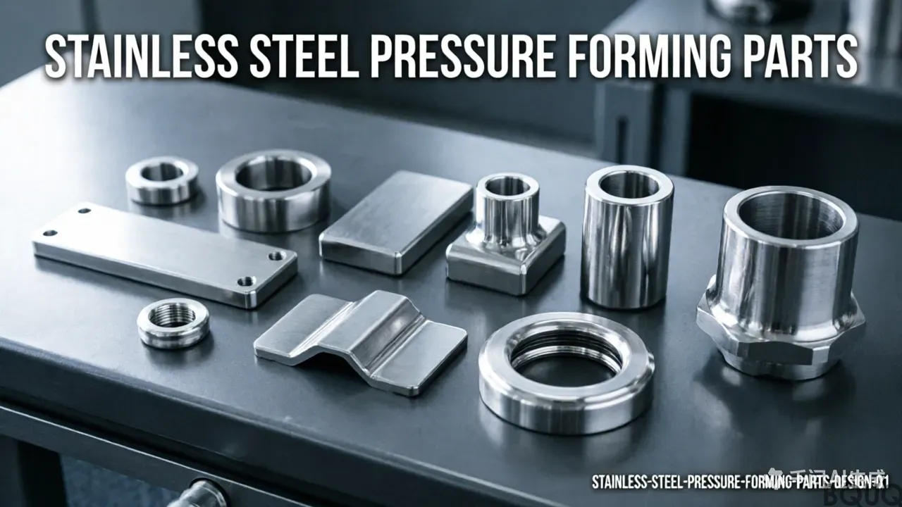
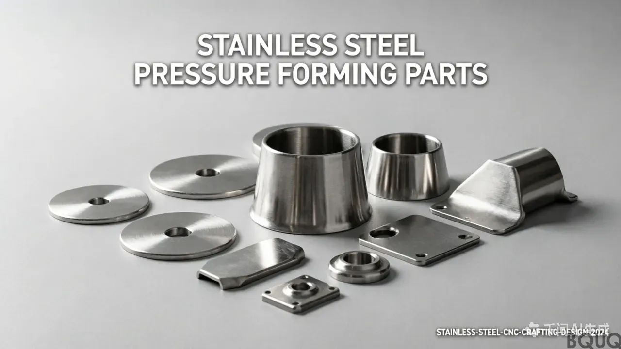
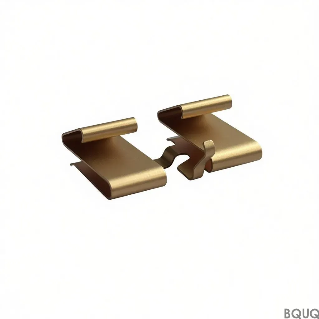
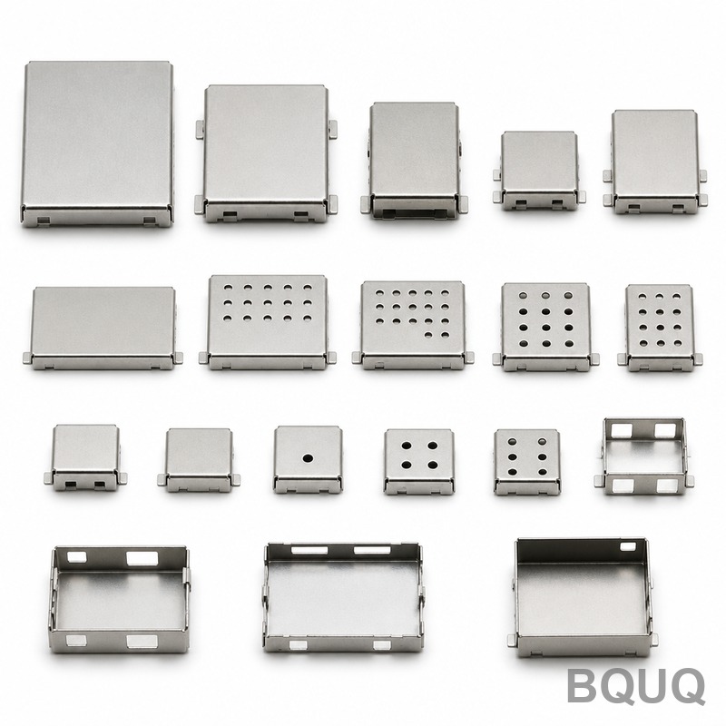
For spring contacts requiring high cycle life (over 10,000 insertions), we recommend copper-nickel-tin alloys like C72650, which provide a yield strength of 800 MPa without the toxicity concerns of beryllium. Stainless steel grades 301 and 304 are used for shielding cans and grounding clips, where magnetic permeability must be below 1.05. In all cases, the material thickness ranges from 0.05 mm for fine-pitch contacts to 3.0 mm for power terminals, with a strip width tolerance of ±0.03 mm.
How Tight Can Tolerances Be for Stamped Electronic Parts?
Precision progressive stamping achieves dimensional tolerances of ±0.01 mm for critical features like contact beam widths and terminal tip radii. Non-critical features such as mounting holes and carrier strip edges can be held to ±0.05 mm. For flatness, we can maintain a camber of less than 0.05 mm over a 100 mm length, essential for surface-mount technology (SMT) connectors. The positional accuracy between the first and last station on a 20-station progressive die is typically ±0.015 mm.
These tight tolerances require a die material of either D2 tool steel hardened to 60-62 HRC or carbide (WC-Co) for runs exceeding 500,000 parts. Carbide dies maintain dimensional stability for over 2 million strokes, whereas D2 steel requires re-grinding after 300,000 strokes. Burr height, a common defect, must be controlled to less than 10% of the material thickness, for example, 0.008 mm maximum burr on 0.08 mm thick stock. We verify these specifications using a coordinate measuring machine (CMM) with a resolution of 0.001 mm.
Why Is Plating Applied Before or After the Stamping Process?
Plating strategy depends on whether the bend radius exposes the base metal. For selectively plated contacts, we plate the strip before stamping, using a spot-plating process that deposits gold (0.76 µm) or palladium-nickel (0.5 µm) only on the contact area. This reduces gold usage by up to 80% compared to barrel plating. However, pre-plated material risks cracking at the bend radius; if the inside bend radius is less than 1.5 times the material thickness, we recommend stamping first and then applying selective brush plating to the formed contact.
Post-stamp plating, such as tin-lead (Sn 90/Pb 10) or matte tin, provides a uniform 2.5 to 5.0 µm coating over the entire part, including sheared edges. This is critical for preventing copper diffusion through the tin layer, which causes oxidation at temperatures above 110°C. The plating adhesion must pass a 180-degree bend test without flaking, per ASTM B571. For automotive applications (USCAR-2), the connector must withstand 1,000 hours of salt spray testing at 35°C with no white corrosion products on the contact surface.
How Much Does Tooling Cost for a New Connector Stamping Project?
Tooling costs scale with the number of stations and geometric complexity. A simple two-station die for a basic flat terminal costs between $3,000 and $8,000 USD. A medium-complexity progressive die for a 0.25-inch pitch connector, with 10 to 15 stations including bending and coining, ranges from $12,000 to $25,000 USD. High-precision dies for fine-pitch (0.3 mm) connectors with 20+ stations, carbide inserts, and in-die tapping cost $40,000 to $80,000 USD. Lead time for tooling is 3 to 5 weeks for simple dies and 8 to 12 weeks for complex carbide dies.
| Parameter | Simple Terminal | Standard Connector | High-Precision Fine-Pitch |
| Number of Stations | 2-4 | 8-12 | 18-25 |
| Tooling Cost (USD) | $3,000-$8,000 | $12,000-$25,000 | $40,000-$80,000 |
| Tolerance (±mm) | 0.05 | 0.02 | 0.01 |
| Minimum Material Thickness (mm) | 0.25 | 0.10 | 0.05 |
| Production Speed (SPM) | 300-600 | 800-1,200 | 400-800 |
| Typical Die Life (strokes) | 500,000 (D2 steel) | 2,000,000 (Carbide) | 5,000,000 (Carbide) |
| Lead Time (weeks) | 3-4 | 5-7 | 10-12 |
What Quality Control Measures Are Required for Electronic Contacts?
Every production lot must be subjected to in-process and final inspection using statistical process control (SPC). We measure critical dimensions, such as contact resistance (must be below 20 mΩ for gold-plated contacts) and insertion force (typically 0.5 to 2.0 N per contact). We utilize a Tektronix micro-ohmmeter for resistance testing and a digital force gauge for insertion/withdrawal forces. X-ray fluorescence (XRF) analysis confirms plating thickness within ±10% of the specification.
For high-reliability applications (medical, aerospace), we perform 100% automated optical inspection (AOI) using a vision system with a 10-megapixel camera, detecting burrs, scratches, and discoloration at a rate of 1,000 parts per minute. Environmental stress screening includes thermal shock testing from -55°C to +125°C for 500 cycles. In addition, we sample parts for salt spray resistance (5% NaCl, 35°C, 48 hours) and humidity testing at 85% RH and 85°C for 1,000 hours per IEC 60068-2-78. All calibration certificates for gauges are traceable to NIST standards.
How Does Part Quantity Affect the Unit Price?
Unit price is inversely proportional to volume due to the amortization of tooling and setup costs. For a typical 0.64mm terminal, the piece price at 100,000 units is approximately $0.08, dropping to $0.03 at 1 million units, and $0.02 at 10 million units. This excludes material surcharges (copper prices fluctuate daily) and plating costs. Setup time for a progressive die is 30 to 60 minutes per tool, which becomes negligible at high volumes but significant for small batches. For low-volume prototype runs (under 5,000 parts), we recommend using a simplified die or wire EDM to produce parts, at a cost of $0.50 to $2.00 per piece.
To optimize costs, we advise grouping multiple similar parts into a single family die, which reduces tooling costs by 30% compared to individual dies. Additionally, using a higher-cost, longer-life carbide die is economically justified when the total run exceeds 2 million parts, as the tooling cost per part becomes negligible and the reduced downtime for sharpening increases throughput by 15%.
Can Metal Stamping Handle Complex 3D Geometries?
Yes, modern multi-axis progressive dies can form complex 3D geometries, including closed-bottom terminals, J-hooks, and box-shaped contacts, without secondary operations. By combining 90-degree bends, coining, and side-cam actions, we can achieve geometries with a height-to-width ratio of up to 3:1. However, there are limitations: the minimum bend radius must be at least 0.5 times the material thickness to prevent cracking, and undercuts are not possible without complex sliding cam mechanisms, which increase tooling cost by 40%.
For extremely complex geometries that cannot be stamped in one piece, we recommend a two-piece assembly. For example, a power connector terminal can be stamped as a flat blank and a separate spring clip, then laser-welded together with a positional accuracy of ±0.05 mm. This hybrid approach maintains the speed of stamping while achieving the geometric freedom of assembly. In-die riveting and tapping are also available, adding threads of M1.0 to M3.0 directly within the stamping press at 200 strokes per minute.
What Are the Common Failure Modes in Stamped Connectors?
The primary failure modes are stress relaxation, fretting corrosion, and hydrogen embrittlement. Stress relaxation occurs when the contact beam loses its normal force at elevated temperatures; for beryllium copper, the loss is 10% after 1,000 hours at 200°C, but for phosphor bronze, the loss is 25%. To mitigate this, we specify a higher initial contact force (over-design by 20%) and choose alloys with higher yield strength. Fretting corrosion happens due to micro-motion at the contact interface; applying a lubricant with a coefficient of friction of 0.15 reduces this by 50%.
Hydrogen embrittlement is a risk when plating high-strength steel (above 1,000 MPa). We mitigate this by baking parts at 190°C for 4 hours after plating, per ASTM B850. Additionally, we monitor the sheared edge quality; excessive burrs can cause arcing and short circuits in high-voltage applications. The die maintenance schedule includes a full inspection every 50,000 strokes, where we check punch and die clearance, which should be 5-8% of material thickness per side.
FAQ
What Is the Minimum Order Quantity for Stamped Electronic Parts?
The minimum order quantity is typically 50,000 pieces for standard progressive stamping, but we offer low-volume production of 5,000 pieces using simplified tooling. For prototypes under 1,000 pieces, we utilize wire EDM, which adds a one-time engineering cost of $300 to $500.
How Fast Can I Get a Quote for a Connector Stamping Project?
We provide a preliminary quote within 12 hours of receiving your 2D drawings or 3D models (STEP or IGES files). A final quote, including tooling and piece price, is confirmed within 24 hours after our engineering review of tolerances and material specifications.
What Is the Maximum Part Size for Progressive Die Stamping?
The maximum part width is 300 mm, and the length is 500 mm, with a maximum material thickness of 5.0 mm. For larger parts, we switch to transfer stamping, which handles parts up to 600 mm square but operates at a slower speed of 50 strokes per minute.
Do You Provide Certifications for Automotive or Medical Applications?
Yes, we are IATF 16949 and ISO 13485 certified. We provide PPAP Level 3 documentation, including material certificates (EN 10204 3.1), CMM reports, and plating thickness certifications for every batch.
Can You Stamp Parts with Nickel Silver or Other Exotic Alloys?
Yes, we work with nickel silver (C75200), copper-nickel (C70600), and Kovar (ASTM F15) for hermetic seals. These materials require slower stamping speeds (200-300 SPM) due to hardness, and tooling may require coated inserts (TiN or CrN) to prevent galling.
How Do You Handle Lead-Free Compliance for Electronic Contacts?
We use lead-free alloys exclusively, such as C11000 with matte tin plating (Sn 99.9%), which is compliant with RoHS and REACH. Our plating lines are certified to ensure the tin does not contain whisker-inducing brighteners, and we perform whisker growth testing per JESD22-A121 for 4,000 hours.
Conclusion
Metal stamping for electronics requires a precise balance of material science, die engineering, and process control to deliver reliable terminals and contacts. Choosing the correct alloy, specifying realistic tolerances, and understanding plating constraints will optimize both performance and cost. For your next connector project, consider a progressive die stamping approach to achieve high volume with repeatable quality.
For a detailed feasibility analysis and a quote within 12 hours, send your drawings to our engineering team. We offer free DFM feedback to reduce tooling costs and improve manufacturability.
| Email: sc@bquq.com | WhatsApp: +86 13713157787 | www.bquq.com |