BQUQ stamps phone and wearable parts from 0.05–0.5 mm strip: contacts, clips, shields, brackets. 0.02–0.05 mm, ISO9001 Dongguan factory, 12-hour quotes.
Stamped Parts for Phones and Wearables: Small, Thin and Precise
Short answer: phone and wearable stamped parts are small, thin metal components produced by progressive dies from coil strip 0.05–0.5 mm thick — battery contacts, shield cans, antenna clips, snap domes, charging pogo retainers and watch-case brackets among them. Blanked features hold ±0.02–0.05 mm and formed features ±0.05 mm, at press speeds of 300–800 strokes per minute. A micro progressive die typically costs $3,000–$15,000, after which per-part prices commonly fall below $0.05. The real engineering challenge is not making the parts small — it is keeping thin strip flat, burr low and plating intact across millions of pieces.
Walk into any phone repair shop and you will see the stamped parts spread across the bench: the stainless shield that covers the main IC, the bent phosphor-bronze contact that feeds the battery, the tiny clip that holds the antenna spring in place. They are easy to overlook and hard to make well. This guide explains how these parts are designed and produced, what tolerances are real at production volumes, and how to source them from a factory that actually runs the process — from our progressive-die lines in Dongguan, where we stamp precision parts alongside CNC, spring and heat sink production under one roof.
What Gets Stamped Inside a Phone or Wearable
The list is longer than most buyers expect. Battery contacts and connector terminals carry power, shield cans and frames contain RF noise, antenna and grounding clips make spring-loaded contact with the chassis, snap domes sit under buttons, SIM trays and camera brackets provide structure, and charging contacts on earbud cases and smartwatches survive thousands of insertions. What unites them is geometry: they are two-and-a-half-dimensional — a flat blank with a few bends — which is exactly the shape a progressive die produces most cheaply.
| Component family | Typical material | Strip thickness | Dominant requirement |
|---|---|---|---|
| Shield cans and frames | Stainless 301, 304 | 0.10–0.20 mm | Flatness, solderability, EMI performance |
| Battery and charging contacts | Phosphor bronze C5210 | 0.08–0.15 mm | Conductivity, contact force, plating adhesion |
| Antenna and grounding clips | Beryllium copper, 301 stainless | 0.05–0.12 mm | Spring force, low resistance, fatigue life |
| Snap domes | 301 stainless, full hard | 0.04–0.10 mm | Dome height, click feel, cycle life |
| Trays, brackets, frames | 304 stainless | 0.20–0.40 mm | Stiffness, hole pattern accuracy, finish |
Each family optimizes a different property. A shield must sit flat for reflow soldering; a battery contact must keep grams of force at the right height after thousands of deflection cycles; a snap dome must click at a predictable ratio of travel. When a buyer sends us a drawing that says only "stamped metal part, stainless," we cannot know which of these the part must do — so the first question we ask is what the part does in the assembly, not what it is called.
How Thin Is Thin? Strip Gauges and the Handling Problem
Phones and wearables push strip thickness down to where the material itself becomes the tolerance problem. Most of these parts run in the 0.05–0.5 mm range, and the coil mill's own gauge tolerance matters: on 0.1 mm strip, thickness typically varies by ±0.005–0.01 mm from the nominal, and that variation flows directly into contact force, spring rate and bend accuracy. Mills supply thin strip in controlled tempers — 301 stainless in 1/2H, 3/4H or full hard, for example — and the temper choice changes the part more than any die feature does. A full-hard 301 strip used for a grounding clip can reach yield strengths around 1,400 MPa; the same material in annealed condition would take a permanent set on the first deflection.
Thin material also changes how the die and press must behave. Carbide die sections, precision guide posts and high-speed presses running 300–800 strokes per minute are standard because the parts are too small and too numerous to run slowly. Stripping the finished part off the punch without bending it takes engineered ejectors, air blow-off or oil jets. Burr control gets harder as thickness drops — burr height is typically held to about 10% of strip thickness and must sit on the side you specify, because on a 0.1 mm part a 0.02 mm burr is a functional defect, not a cosmetic one. Flatness and warp are managed with strip tension, leveling passes and coining stations, not by hoping the material behaves.
| Parameter | Realistic production range on 0.05–0.5 mm strip |
|---|---|
| Strip thickness commonly stamped | 0.05–0.50 mm; special runs to ~0.03 mm |
| Blanked profile and hole position | ±0.02–0.05 mm |
| Formed dimensions | ±0.05 mm with coining where needed |
| Minimum hole diameter | ~0.8–1.0× strip thickness; 0.15–0.20 mm practical in production |
| Minimum inside bend radius | 0.5–1.0× thickness (ductile); 1.0–2.0× (spring temper) |
| Burr height | ≤10% of thickness, on the specified side |
The Tolerances That Actually Matter on Tiny Parts
Buyers tend to put one blanket tolerance on the whole drawing. On small stamped parts, three different kinds of accuracy matter and they are held by different means. Flat blanked geometry — profiles, holes, slots — is held by the die's punch-and-die clearance and guide precision, routinely ±0.02–0.05 mm. Formed geometry — bends, heights, angles — is held by material temper consistency and die compensation for springback, realistically ±0.05 mm and ±0.5–1.0° on angles. Position across the strip — pitch and hole-to-hole location — is held by the press feed and pilot pins, typically ±0.03–0.05 mm over a part's length.
For surface-mount parts there is a fourth number that is not on most drawings but decides whether assembly works: coplanarity. Connector contacts and SMT shields must land flat enough for solder paste contact, and a coplanarity spec of 0.05–0.10 mm across the part is common. This is measured with optical systems or a CMM on a fixture, not with calipers. When we quote a small stamped part we state which features are measured, with what, and how often during the run, because a tolerance nobody verifies is a tolerance nobody holds. First-article reports at tool tryout, in-process checks during the run, and a dimensional report with every batch are standard practice on our precision metal stamping services line.
Designing Thin Parts for the Die: Rules That Save Money
Most cost in micro stamping is engineered in before the die is cut. Follow the rules that thin-strip stamping is built around and the tool is cheaper, the press runs faster, and yields stay high. Inside bend radii below about 0.5–1.0× thickness on ductile materials — and 1–2× on spring temper — cause cracking at the bend line and should be opened or avoided. Keep holes and slots at least one thickness away from edges and bends where possible, because metal displaced by a nearby bend flows into the hole and distorts it. Where a spring beam must flex, orient it across the strip's grain direction when the layout allows, because bend and flex performance follow the rolling direction. And design in symmetry: a part that is symmetric left-to-right bends with balanced forces and stays flatter than a part that pulls to one side.
Springback deserves its own paragraph because it is the difference between a die that works and a die that fights. When the punch releases, the material springs back toward its original shape; the amount depends on thickness, temper, bend radius and bend angle. Die makers compensate with overbend angles, coining the bend zone to yield the material locally, or both — and the correction is validated at tool tryout, not guessed in design. This is why the first article from a new die is so important: it is the moment measured reality replaces calculated expectation. A factory that stamps precision-stamped contact springs and watch parts every day accumulates exactly this compensation data, which is why parts that look similar to ones we have already tooled come out right faster.
Plating and Finish: Doing It Right on Thin Strip
Most phone and wearable stamped parts are plated, and the sequence — plate the strip before forming, or form then plate the part — is a real design decision. Pre-plated strip is common for contacts and terminals: the coil arrives with selective gold, tin or nickel already applied in the exact zones needed, and the die never touches plated edges that would wear the finish. The tradeoff is that forming a pre-plated strip can crack brittle platings at tight bend radii, so the minimum radius rules above get stricter when plating is involved. Post-forming barrel or rack plating covers everything, including the raw edge of the blank, which matters for corrosion on cut edges but can also plate surfaces where you do not want metal-to-metal friction, like a contact wipe zone.
Typical finishes on these parts are a nickel underlayer with selective gold flash of roughly 0.05–0.5 µm on contact areas, tin or tin-lead-free finishes on solderable shields and terminals, and bare passivated stainless where corrosion resistance is the goal. Plating thickness on the functional surface should be specified in microns on the drawing, not as "gold plated," because a flash coat and a wear-grade deposit are different products at different prices. When the contact carries current and must survive years of duty cycles, the material and plating spec deserve the same rigor as the geometry — details that our stamped terminal design guide covers in depth.
Prototyping Before Committing to a Full Die
A production progressive die is a $3,000–$15,000+ decision that you should not make on the first design iteration. The lower-risk path is a prototype stage: parts cut and formed by soft tooling, CNC machining of blanks with hand or press forming, or a simplified single-station tryout die that validates material, bend radii and function before the full multi-stage tool is cut. Prototype quantities of a few hundred to a few thousand parts let you test contact force, fit in the actual housing and plating behavior, and change the design while changes are still cheap. Expect prototype samples typically within two to four weeks of drawing approval, and a production tool — depending on stage count — a few weeks beyond that.
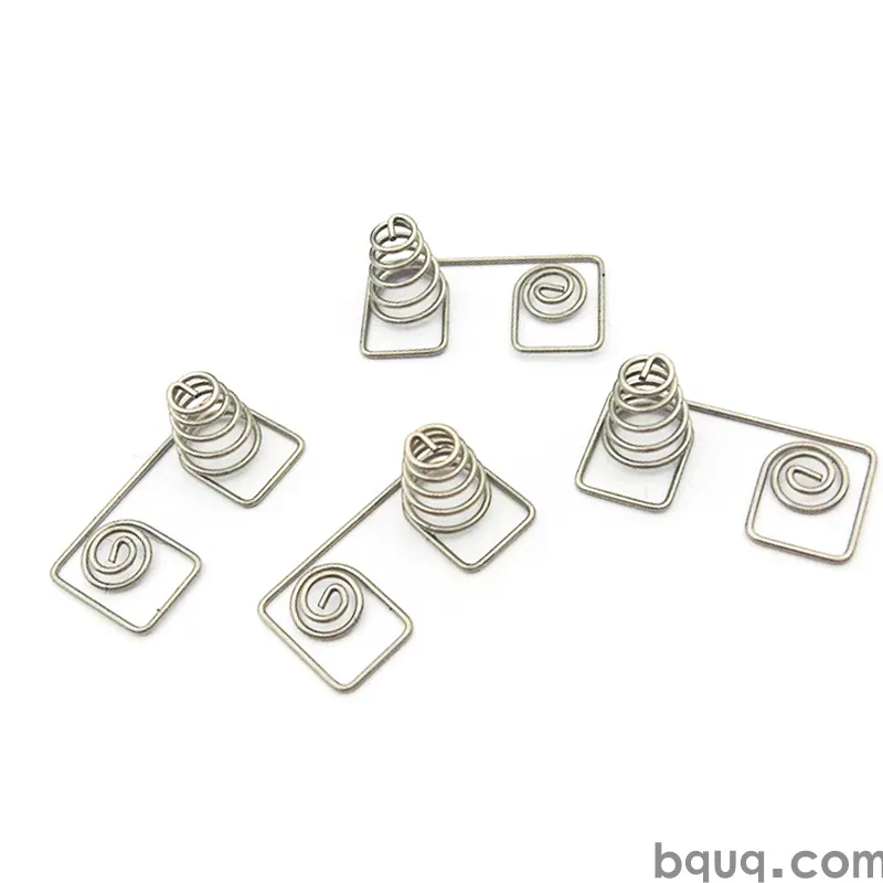
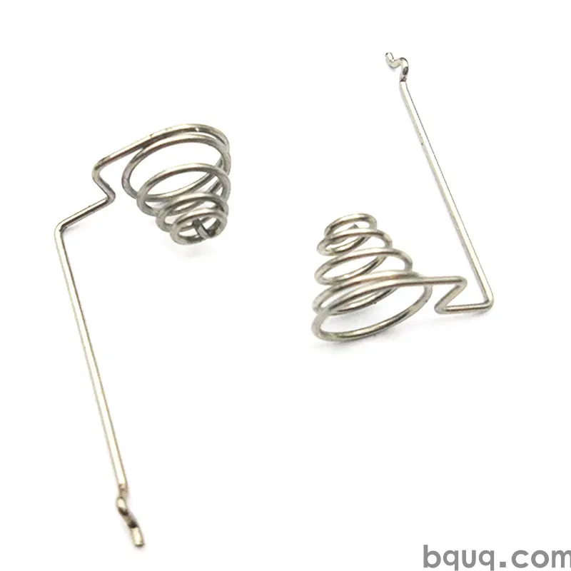
Many wearable assemblies also pair a stamped contact with a wound coil spring — the side contact in a battery holder or the pin in a charging puck, for example. When a design mixes stamped and wound elements, it pays to have one engineering conversation across both, which is exactly what a factory running micro springs and stamping lines together can do. When you send your drawing to sc@bquq.com or WhatsApp +86 13713157787, tell us the annual volume as well as the geometry: it decides whether we quote a multi-out production die, a prototype tool, or an honest recommendation that your part should not be stamped at all yet.
Frequently Asked Questions
Q: How thin can a stamped phone or wearable part be?
A: Production stamping on thin strip typically starts around 0.05 mm and runs comfortably to 0.5 mm, with some snap domes and foils down to about 0.03 mm. Below 0.05 mm, handling, burr and plating defects dominate yield, so the die and process need to be designed for the thickness rather than adapted to it.
Q: What tolerances can you hold on small stamped parts?
A: Blanked profiles and hole positions hold ±0.02–0.05 mm, formed dimensions ±0.05 mm, and bend angles ±0.5–1.0° with coining stations. Coplanarity on surface-mount parts is typically specified at 0.05–0.10 mm. Tighter callouts raise die cost and slow the press, so we flag dimensions that do not need it.
Q: Do stamped parts need plating, and can you plate selectively?
A: Plating depends on function: contacts usually need a nickel underlayer with selective gold on the wipe zone, while solderable shields take tin finishes. Selective plating of thin strip in defined zones is standard. Specify the finish in microns on the drawing and we will confirm what is achievable on your part.
Q: How many pieces justify a progressive die for a wearable part?
A: Roughly 50,000 pieces per year and up makes a progressive die economical for most micro parts, because a $10,000 tool adds $0.20 per part at 50,000 pieces but only $0.01 at a million. Below that volume, prototype tooling, CNC-formed blanks or photo etching are usually the honest recommendation.
Q: Should plating happen before or after forming?
A: Both are used. Pre-plated strip gives clean selective plating but can crack at tight bends, so minimum bend radii must be respected. Post-forming plating covers cut edges for corrosion but plates everything unless masked. We recommend the sequence based on your material, bend geometry and corrosion requirements.
Related Resources
- Precision metal stamping services in China: capabilities, tolerances and lead times for small stamped parts from a Dongguan source factory.
- Stamped terminals and contacts: progressive-die production of the small conductive parts inside phones and wearables.
- About BQUQ: an ISO9001-certified source factory running stamping, CNC, spring and heat sink lines under one roof.
- Contact us: send the drawing for a quote within 12 working hours.
Authored by the BQUQ Engineering Team. BQUQ is an ISO9001-certified source factory in Dongguan, China, running CNC machining, metal stamping, custom springs, heat sink and collet lines under one roof. Send drawings to sc@bquq.com or WhatsApp +86 13713157787 for a quote within 12 working hours. www.bquq.com